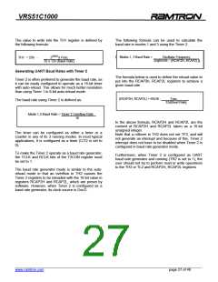
VRS51C1000
UART Operation in Mode 1
UART Transmission in Mode 1
Transmission in this mode is initiated by any
instruction that makes use of SBUF as a destination
register. The 9th bit position of the transmit shift register
is loaded by the “write to SBUF” signal. This event also
flags/informs the TX Control Unit that a transmission
has been requested.
In Mode 1 operation, 10 bits are transmitted (through
TXD) or received (through RXD). The transactions are
composed of: a Start bit (Low); 8 data bits (LSB first)
and one Stop bit (high). The reception is completed
once the Stop bit sets the RB8 flag in the SCON
register. Either Timer 1 or Timer 2 controls the baud
rate in this mode.
It is after the next rollover in the divide-by-16 counter
when transmission actually begins. It follows that the
bit times are synchronized to the divide-by-16 counter
and not to the “write to SBUF” signal.
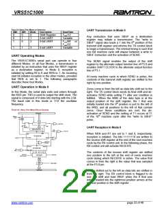
The following diagram shows the serial port structure
when configured in Mode 1.
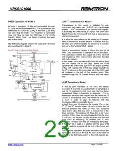
FIGURE 17: SERIAL PORT MODE 1 AND 3 BLOCK DIAGRAM
When a transmission begins, it places the start bit at
TXD. Data transmission is activated one bit time later.
This activation enables the output bit of the transmit
shift register to TXD. One bit time after that, the first
shift pulse occurs.
In this Mode, zeros are clocked in from the left as data
bits are shifted out to the right. When the most
significant bit of the data byte is at the output position
of the shift register, the 1 that was initially loaded into
the 9th position is to the immediate left of the MSB, and
all positions to the left of that contain zeros. This
condition flags the TX Control Unit to shift one more
time.
Internal Bus
1
Write to
SBUF
Timer 1
Overflow
Q
S
D
SBUF
TXD
CLK
Timer 2
Overflow
ZERO DETECTOR
÷2
0
1
Shift
Start
Data
SMOD
0
0
1
TX Control Unit
TCLK
TX Clock
÷16
Send
÷16
TI
1
RCLK
Serial Port
Interrupt
RI
RX Clock
Load
SBUF
RX Control Unit
1-0 Transition
Detector
Start
SHIFT
UART Reception in Mode 1
A one to zero transition at pin RXD will initiate
reception. It is for this reason that RXD is sampled at a
rate of 16 multiplied by the baud rate that has been
established. When a transition is detected, 1FFh is
written into the input shift register and the divide-by-16
counter is immediately reset. The divide-by-16 counter
is reset in order to align its rollovers with the
boundaries of the incoming bit times.
Bit
Detector
9-Bit Shift Register
Shift
RXD
LOAD SBUF
SBUF
READ SBUF
Internal Bus
In total, there are 16 states in the counter. During the
7th, 8th and 9th counter states of each bit time; the bit
detector samples the value of RXD. The accepted
value is the value that was seen in at least two of the
three samples. The purpose of doing this is for noise
rejection. If the value accepted during the first bit time
is not zero, the receive circuits are reset and the unit
goes back to searching for another one to zero
transition. All false start bits are rejected by doing this.
If the start bit is valid, it is shifted into the input shift
register, and the reception of the rest of the frame will
proceed.
For a receive operation, the data bits come in from the
right as 1’s shift out on the left. As soon as the start bit
arrives at the leftmost position in the shift register, (9-
______________________________________________________________________________________________
www.ramtron.com page 23 of 48

 RAMTRON [ RAMTRON INTERNATIONAL CORPORATION ]