HYB18H512321AF
512-Mbit GDDR3
Electrical Characteristics
5.13
AC Timings ( HYB18H512321AFL14/16/20)
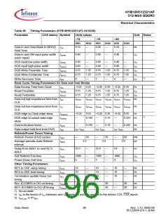
Table 39
Timing Parameters (HYB18H512321AFL14/16/20)
Parameter
CAS latency Symbol
Limit values
–14
Unit Notes
–16
–20
min
max min
max min
max
Clock and Clock Enable
3501)
3501)
3501)
3501)
3501)
0.45
700
650
600
500
450
0.55
0.55
—
3501) 600
3501) 550
3501) 500
3501) 450
3501) 400
MHz
System frequency
CL = 11
fCK11
fCK10
fCK9
fCK8
fCK7
tCH
3501)
3501)
3501)
3501)
0.45
0.45
0.45
500
450
400
350
0.55
0.55
—
MHz
MHz
MHz
MHz
tCK
CL = 10
CL = 9
CL = 8
CL = 7
0.45
0.45
0.45
0.55
0.55
—
Clock high level width
Clock low level width
Minimum clock half period
0.45
tCK
tCL
tHP
2)
0.45
tCK
Command and Address Setup and Hold Timing
0.35
—
0.4
—
0.5
—
ns
Address/Command input setup
tIS
time
0.35
0.7
—
—
0.4
0.7
—
—
0.5
0.7
—
—
ns
Address/Command input hold time tIH
tCK
Address/Command input pulse
tIPW
width
Mode Register Set Timing
6
—
—
6
—
—
6
—
—
tCK
tCK
Mode Register Set cycle time
Mode Register Set to READ timing tMRDR
tMRD
12
12
12
Row Timing
Row Cycle Time
Row Active Time
ACT(a) to ACT(b) Command period tRRD
Row Precharge Time
Row to Column Delay Time for
Reads
30
18
7
—
—
—
—
—
27
17
6
—
—
—
—
—
23
14
5
—
—
—
—
—
tCK
tCK
tCK
tCK
tCK
tRC
tRAS
3)
5)
12
11
11
10
9
tRP
8
tRCDRD
tRCDWR(min) = tRCDRD(min) - (WL + 1) × tCK
tCK
Row to Column Delay Time for
Writes
tRCDWR
Column Timing
CAS(a) to CAS(b) Command
period
Write to Read Command Delay
Read to Write command delay
4)
2
5
—
—
2
5
—
—
2
4
—
—
tCK
tCCD
5)
6)
tCK
tCK
tWTR
tRTW(min)= (CL + BL/2 +2 -WL)
tRTW
Write Cycle Timing Parameters for Data and Data Strobe
WL–
WL+0. WL–
25
WL+0 WL -
WL
+0.25
tCK
Write command to first WDQS
tDQSS
0.25
0.25
.25
0.25
latching transition
0.18
—
0.20
—
0.24
—
ns
Data-in and Data Mask to WDQS tDS
Setup Time
Data Sheet
95
Rev. 1.73, 2005-08
05122004-B1L1-JEN8

 QIMONDA [ QIMONDA AG ]