HYB18H512321AF
512-Mbit GDDR3
Electrical Characteristics
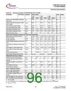
Table 39
Timing Parameters (HYB18H512321AFL14/16/20)
Parameter
CAS latency Symbol
Limit values
–14
Unit Notes
max
–16
–20
max min
min
max min
0.18
—
0.20
—
0.24
—
ns
Data-in and Data Mask to WDQS tDH
Hold Time
0.40
—
0.40
—
0.40
—
tCK
Data-in and DM input pulse width tDIPW
(each input)
0.40
0.40
0.75
0.75
8
—
0.40
0.40
0.75
0.75
7
—
0.40
0.40
0.75
0.75
6
—
tCK
tCK
tCK
tCK
tCK
DQS input low pulse width
DQS input high pulse width
DQS Write Preamble Time
DQS Write Postamble Time
Write Recovery Time
tDQSL
tDQSH
tWPRE
tWPST
tWR
—
—
—
1.25
1.25
—
1.25
1.25
—
1.25
1.25
—
7)
Read Cycle Timing Parameters for Data and Data Strobe
–0.25
0.25
1.25
1.25
–0.28 0.28
–0.35 0.35
ns
Data Access Time from Clock
tAC
0.75
0.75
0.75
1.25
1.25
0.75
0.75
1.25
1.25
tCK
tCK
Read Preamble
tRPRE
0.75
Read Postamble
tRPST
tACmin
tACmax tACmin tACmax tACmin
tACmax ns
Data-out high impedance time from tHZ
CLK
tACmin
tACmax tACmin tACmax tACmin
tACmax ns
Data-out low impedance time from tLZ
CLK
–0.25
—
0.25
–0.28 0.28
–0.35 0.35
ns
DQS edge to Clock edge skew
DQS edge to output data edge
skew
tDQSCK
tDQSQ
7)
0.160
—
0.18
—
0.225 ns
—
0.160
—
0.18
—
0.225 ns
ns
Data hold skew factor
tQHS
tQH
tHP–tQHS
tHP–tQHS
tHP–tQHS
Data output hold time from DQS
Refresh/Power Down Timing
Refresh Period (8192 cycles)
Average periodic Auto Refresh
interval
—
32
—
—
32
—
—
32
—
ms
µs
tREF
tREFI
3.9
3.9
3.9
52.0
52.8
54
ns
Delay from AREF to next ACT/
AREF
tRFC
1000
6
—
—
1000
5
—
—
1000
4
—
—
tCK
tCK
Self Refresh Exit time
tXSC
tXPN
Power Down Exit time
Other Timing Parameters
RES to CKE setup timing
RES to CKE hold timing
Termination update Keep Out
timing
10
10
10
—
—
—
10
10
10
—
—
—
10
10
10
—
—
—
ns
ns
ns
tATS
tATH
tKO
—
—
20
20
—
—
20
20
—
—
20
20
ns
ns
Rev. ID EMRS to DQ on timing
REV. ID EMRS to DQ off timing
1) DLLon mode
tRIDon
tRIDoff
2) tHP is the lesser of tCL minimum and tCH minimum actually applied to the device CLK, CLK inputs
3) tRAS,max is 8*tREFi
Data Sheet
96
Rev. 1.73, 2005-08
05122004-B1L1-JEN8

 QIMONDA [ QIMONDA AG ]