RELEASED
PM7350 S/UNI DUPLEX
DATA SHEET
PMC-1980581
ISSUE 8
DUAL SERIAL LINK PHY MULTIPLEXER
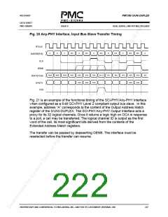
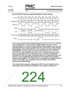
Fig. 20 Any-PHY Interface, Input Bus Slave Transfer Timing
IFCLK
A
B
C
3Fh
D
3Fh
A
3Fh
B
3Fh
C
3Fh
3Fh
A
IADDR[5:0]
ICA
IENB
W 24
W 25
W 26
W 27
XXX
XXX
XXX
XXX
XXX
XXX
CH D
W 1
W 2
W 3
XXX
XXX
XXX
XXX
W 3
IDAT[15:0]
IPRTY
ISX
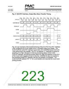
Fig. 21 is an example of the functional timing of the SCI-PHY/Any-PHY Interface
when configured as a 8-bit SCI-PHY Level 2 compliant output bus slave. In this
example, address “A” corresponds to the content of the Output Address Match
register of the S/UNI-DUPLEX. The SCI-PHY/Any-PHY Output Interface acts a
proxy for its 32 logical channels. Once it returns a logic high on OCA in response
to a poll, a cell may be transferred. The logical channel ID is output as the first
word of the cell, its most significant bits derived from the contents of the
Extended Address Match registers.
The transfer can be paused by deasserting OENB. The interface must be
reselected before the transfer can resume.
PROPRIETARY AND CONFIDENTIAL TO PMC-SIERRA, INC., AND FOR ITS CUSTOMERS’ INTERNAL USE
207

 PMC [ PMC-SIERRA, INC ]