RELEASED
PM7350 S/UNI DUPLEX
DATA SHEET
PMC-1980581
ISSUE 8
DUAL SERIAL LINK PHY MULTIPLEXER
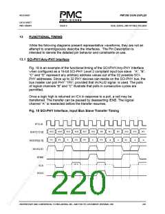
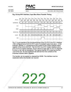
Fig. 19 gives an example of the functional timing of the SCI-PHY/Any-PHY
Interface when configured as a 16-bit SCI-PHY Level 2 compliant input bus
master. When polling PHY devices, the S/UNI-DUPLEX inserts null cycles by
deasserting the IAVALID output and forcing the IADDR[4:0] bus to “1Fh” to
prevent bus contention. Once a ready to transfer PHY is found (PHY at address
“C” in this example), its address is maintained on the address bus till the current
transfer is completed. The PHY is then selected and the transfer initiated. The
S/UNI-DUPLEX transfers the complete cell without pause.
Fig. 19 SCI-PHY Interface, Input Bus Master Transfer Timing
IFCLK
XXX
W 20
A
W 21
IFh
W 22
B
W 23
1Fh
W 24
C
W 25
1Fh
W 26
XXX
1Fh
W 0
D
W 1
IDAT[15:0]
IADDR[4:0]
IAVALID
IENB
1Fh
C
CH C
ICA
ISOC
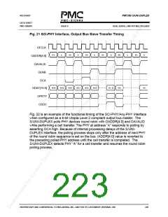
Fig. 20 gives an example of the functional timing of the of the SCI-PHY/Any-PHY
Interface when configured as a 16-bit Any-PHY compliant input bus slave. In this
example, the IAVALID pin is used as the IADDR[5] line of the IADDR[5:0] bus
(the null address becomes 3Fh) and the Extended Address register is
unused.The polls of logical channels “A”, “B” and “C” illustrate that polls in
consecutive cycles are permitted. The S/UNI-DUPLEX responds to polling of
logical channel “D” by asserting ICA high on the second following clock cycle.
Logical channel “D” is selected by the bus master assertion of ISX and a cell
transfer is initiated. The IENB input is not required to be deasserted at the end of
a cell transfer. Upon completion of the cell transfer, the interface autonomously
deselects itself.
The transfer can be paused by deasserting IENB. The cell transfer from the same
logical channel resumes immediately when IENB is reasserted low.
PROPRIETARY AND CONFIDENTIAL TO PMC-SIERRA, INC., AND FOR ITS CUSTOMERS’ INTERNAL USE
206

 PMC [ PMC-SIERRA, INC ]