RELEASED
PM7350 S/UNI DUPLEX
DATA SHEET
PMC-1980581
ISSUE 8
DUAL SERIAL LINK PHY MULTIPLEXER
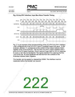
Fig. 23 Any-PHY Interface, Output Bus Slave Transfer Timing
OFCLK
B
A
3Fh
B
3Fh
A
3Fh
3Fh
C
3Fh
D
OADDR[4:0]
OENB
OCA
ODAT[15:0]
W 24
W 25
W 26
W 26
W 27
CH ID
W 1
W 2
W 3
OSX
OSOC
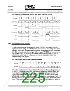
13.2 Clocked Serial Data Interface
The timing relationship of the transmit clock (LTXC[N]) and data (LTXD[N])
signals is shown in Fig. 24. The transmit data is viewed as a contiguous serial
stream. Data bytes are transmitted from most significant bit to least significant
bit. Bits are updated on the rising or falling edge of LTXC[N], as determined be
the value of the LTXCINV bit of the Master Configuration register (in Fig. 24,
LTXCINV is set to logic 0). A transmit link may be stalled by holding the
corresponding LTXC[N] low.
Fig. 24 Clocked Serial Data Transmit Interface
LTXC[N]
LTXD[N]
B[1]
B[0]
B[7]
B[6]
B[5]
B[4]
B[3]
B[2]
When the ALIGN bit of the Transmit Serial Framing Bit Threshold register is set
to logic 1, a clock gap longer that the minimum detectable period causes the
most significant bit of the data octet to be output during the gap period. The
S/UNI-DUPLEX can detect clock gaps of 8 line clock periods over the entire
LTXC[15:0] clock line frequency range. The range of the frequency at which 1 bit
framing gap can be detected changes linearly with the speed of the high-speed
links. When operating the LVDS link at 200 Mb/s (REFCLK frequency set to 25
PROPRIETARY AND CONFIDENTIAL TO PMC-SIERRA, INC., AND FOR ITS CUSTOMERS’ INTERNAL USE
210

 PMC [ PMC-SIERRA, INC ]