RELEASED
PM7350 S/UNI DUPLEX
DATA SHEET
PMC-1980581
ISSUE 8
DUAL SERIAL LINK PHY MULTIPLEXER
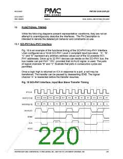
13
FUNCTIONAL TIMING
While the following diagrams present representative waveforms, they are not an
attempt to unambiguously describe the interfaces. The Pin Description is
intended to denote the detailed pin behavior and constraints on use.
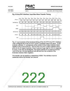
13.1 SCI-PHY/Any-PHY Interface
Fig. 18 is an example of the functional timing of the SCI-PHY/Any-PHY Interface
when configured as a 16-bit SCI-PHY Level 2 compliant input bus slave. “A”, “B”,
“C” and “D” represent any arbitrary address values out of the 32 possible SCI-
PHY addresses. Since up to 32 PHY devices can reside on the SCI-PHY bus, the
bus master can poll PHY “1Fh”, provided that IAVALID signal is used. The polls
of logical channels “B” and “C” illustrate that polls in consecutive cycles are
permitted.
Once a logic high is returned on ICA in response to a poll, a cell may be
transferred. The transfer can be paused by deasserting IENB. The logical
channel “A” is reselected before the transfer resumes.
Fig. 18 SCI-PHY Interface, Input Bus Slave Transfer Timing
IFCLK
XXX
A
W 23
1Fh
W 24
IFh
W 25
A
W 26
1Fh
W 27
1Fh
W 0
W 1
B
W 2
C
XXX
XX
XXX
A
W 3
D
IDAT[15:0]
IADDR[4:0]
IAVALID
IENB
1Fh
CH A
ICA
ISOC
PROPRIETARY AND CONFIDENTIAL TO PMC-SIERRA, INC., AND FOR ITS CUSTOMERS’ INTERNAL USE
205

 PMC [ PMC-SIERRA, INC ]