RELEASED
PM7350 S/UNI DUPLEX
DATA SHEET
PMC-1980581
ISSUE 8
DUAL SERIAL LINK PHY MULTIPLEXER
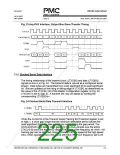
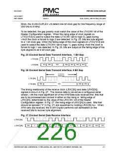
MHz), the S/UNI-DUPLEX will detect one bit clock gap for line frequency range of
200 kHz to 8 MHz.
To be detected, the gap polarity must match the value of the LTXCINV bit of the
Master Configuration register. When the rising edge of clock signals on
LTXC[15:0] is used to output the data (LTXCINV set to logic 0), gaps during
which the clock is forced to logic 0 are detected. In Fig. 25, bits are byte aligned
to a 1 bit clock gap. When the falling edge of the clock signals on LTXC[15:0] are
used to output the data (LTXCINV set to logic 1), gaps during which the clock is
forced to logic 1 are detected. In Fig. 26, bits are output on the falling edge of the
byte aligned to an 8 bit clock gap.
Fig. 25 Clocked Serial Data Transmit Interface, 1 Bit Gap
LTXC[N]
B[1]
B[0]
B[7]
B[6]
B[5]
B[4]
B[3]
LTXD[N]
Fig. 26 Clocked Serial Data Transmit Interface, 8 Bit Gap
8 CLOCK
PERIODS
LTXC[N]
B[0]
B[7]
B[6]
B[5]
LTXD[N]
The timing relationship of the receive clock (LRXC[N]) and data (LRXD[N])
signals is shown in Fig. 27. The receive data is viewed as a contiguous serial
stream, with the most significant bit of the ATM/Data byte received first. Bits that
are to be processed are clocked in either on the rising or falling edge of
LRXC[N], determined by the value of the LRXCINV bit of the Master
Configuration register. In Fig. 27, the rising edge of LRXC[N] is used. Bits that
should be ignored (“X” in Fig. 27) are squelched by holding LRXC[N] low. When
ATM cells are received, the S/UNI Duplex performs cell delineation on the
received bits to recover byte alignment.
Fig. 27 Clocked Serial Data Receive Interface
LRXC[N]
B[5]
X
X
B[4]
B[3]
B[2]
X
B[1]
X
B[0]
B[7]
B[6]
B[5]
LRXC[N]
PROPRIETARY AND CONFIDENTIAL TO PMC-SIERRA, INC., AND FOR ITS CUSTOMERS’ INTERNAL USE
211

 PMC [ PMC-SIERRA, INC ]