PEX 8532 Transparent Mode Port Registers
PLX Technology, Inc.
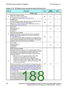
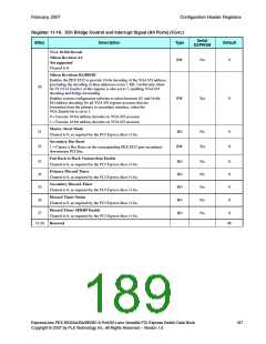
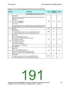
Register 11-16. 3Ch Bridge Control and Interrupt Signal (All Ports) (Cont.)
Serial
EEPROM
Bit(s)
Description
Type
Default
Bridge Control
Parity Error Response Enable
Controls the response to Poisoned TLPs.
16
RW
Yes
0
1 = Enables the secondary Master Data Parity Error bit
SERR# Enable
Controls forwarding of ERR_COR, ERR_FATAL, and ERR_NONFATAL
from the secondary interface to the primary interface.
When set to 1, and the Command register SERR# Enable bit value is 1,
enables the Signaled System Error bit.
17
RW
Yes
No
0
0
ISA Enable
Silicon Revision AA
Not supported
Cleared to 0.
Silicon Revisions BA/BB/BC
18
Modifies the PEX 8532’s response to ISA I/O addresses enabled by the
I/O Base and I/O Limit registers and located in the first 64 KB of the
PCI I/O Address space.
RW
Yes
No
0
0
1 = PEX 8532 blocks forwarding from the primary to secondary interface,
of I/O transactions addressing the last 768 bytes in each 1-KB block. In the
opposite direction (secondary to primary), I/O transactions are forwarded
when they address the last 768 bytes in each 1-KB block.
VGA Enable
Silicon Revision AA
Not supported
Cleared to 0.
Silicon Revisions BA/BB/BC
Modifies the PEX 8532’s response to VGA-compatible addresses. When set,
the bridge on the switch’s appropriate port positively decodes and forwards
the following accesses on the primary to secondary interface (and,
conversely, blocks the forwarding of these addresses from the secondary
to primary interface):
•
•
Memory accesses in the range 000A_0000h to 000B_FFFFh
I/O address in the first 64 KB of the I/O Address space
[Address[31:16] for PCI Express are zero (0000h)] and where
Address[9:0] is within the range of 3B0h to 3BBh or 3C0h to 3DFh
(inclusive of ISA address aliases – Address[15:10] can be any value
and is not used in decoding)
19
RW
Yes
0
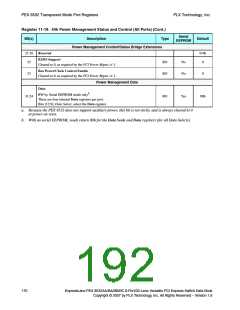
When the VGA Enable bit is set, VGA address forwarding is independent of
the ISA Enable bit value, and the I/O Address range and Memory Address
ranges defined by the I/O Base and I/O Limit, Memory Base Address and
Memory Limit Address, and Prefetchable Memory Base Address and
Prefetchable Memory Limit Address registers. VGA address forwarding
is qualified by the Command register I/O Access Enable and Memory
Access Enable bits.
0 = Does not forward VGA-compatible Memory and I/O addresses from
the primary to secondary interface (addresses defined above), unless they
are enabled for forwarding by the defined I/O and Memory Address ranges
1 = Forwards VGA-compatible Memory and I/O addresses (addresses
defined above) from the primary to secondary interface (when the I/O
Access Enable and Memory Access Enable bits are set), independent
of the I/O and Memory Address ranges and ISA Enable bit
166
ExpressLane PEX 8532AA/BA/BB/BC 8-Port/32-Lane Versatile PCI Express Switch Data Book
Copyright © 2007 by PLX Technology, Inc. All Rights Reserved – Version 1.6

 PLX [ PLX TECHNOLOGY ]