Philips Semiconductors
Preliminary specification
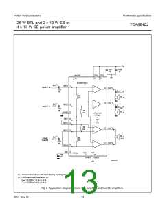
26 W BTL and 2 × 13 W SE or
4 × 13 W SE power amplifier
TDA8512J
12 DC CHARACTERISTICS
VP = 15 V; Tamb = 25 °C; measured according to Figs 6 and 7; unless otherwise specified.
SYMBOL
Supply
PARAMETER
CONDITIONS
MIN.
TYP.
MAX.
UNIT
VP
supply voltage
note 1
6
−
−
−
15
18
V
Iq(tot)
VO
total quiescent current
DC output voltage
80
6.9
−
160
−
mA
V
∆VOO
DC output offset voltage
note 2
150
mV
Mode select switch
Vsw(on)
switch-on voltage
8.5
−
−
V
Mute condition
V
mute voltage
3.3
−
−
−
−
6.4
2
V
VO
output voltage
Vi(max) = 1 V; fi = 1 kHz
note 2
mV
mV
∆VOO
DC output offset voltage
−
150
Standby condition
Vstb
Istb
standby voltage
0
−
−
−
2
V
standby current
−
100
40
µA
µA
Isw(on)
switch-on current
12
Notes
1. The circuit is DC adjusted at VP = 6 to 18 V and AC operating at VP = 8.5 to 18 V.
2. Only for BTL channel (VOUT4 − VOUT3).
13 AC CHARACTERISTICS
VP = 15 V; fi = 1 kHz; Tamb = 25 °C; bandpass 22 Hz to 22 kHz; measured according to Figs 6 and 7; unless otherwise
specified.
SYMBOL
PARAMETER
CONDITIONS
MIN.
TYP.
MAX. UNIT
BTL channel
Po
output power
RL2 = 4 Ω (see Fig.7); note 1
THD = 0.5%
16
20
26
−
W
W
%
THD = 10%
22
−
−
−
THD
BP
total harmonic distortion
power bandwidth
Po = 1 W
0.06
THD = 0.5%; Po = −1 dB with
−
20 to 15000 −
Hz
respect to 17 W
fro(l)
low frequency roll-off
at −1 dB; note 2
at −1 dB
−
25
−
−
Hz
fro(h)
GV
high frequency roll-off
20
25
−
kHz
dB
closed loop voltage gain
supply voltage ripple rejection
26
27
SVRR
note 3;
operating
mute
48
46
80
−
−
−
−
−
−
dB
dB
dB
standby
2001 Nov 16
9

 NXP [ NXP ]