Philips Semiconductors
Preliminary specification
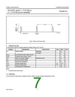
26 W BTL and 2 × 13 W SE or
4 × 13 W SE power amplifier
TDA8512J
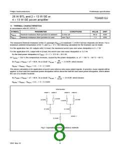
14 APPLICATION INFORMATION
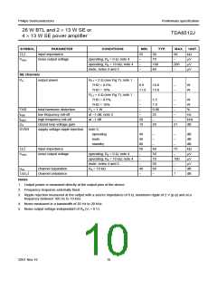
14.1 Input configuration
For suppressing higher frequency transients (spikes) on
the supply line a capacitor with low ESR (typical 0.1 µF)
has to be placed as close as possible to the device. For
suppressing lower frequency noise and ripple signals, a
large electrolytic capacitor (e.g.1000 µF or more) must be
placed close to the device.
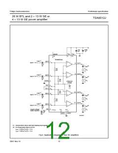
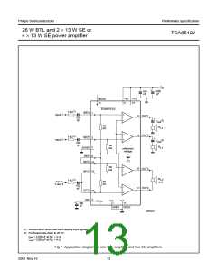
• Inputs 1 and 2 are used for SE application on pin OUT1,
respectively pin OUT2
• Input 3 can be configured for both SE and BTL
application
The bypass capacitor on the pin RR reduces the noise and
ripple on the mid rail voltage. For good THD and noise
performance, a low ESR capacitor is recommended.
• Input 4 can be used for SE application of pin OUT4, or
for BTL application together with input 3. See
Figs 6 and 7.
14.5 Switch-on and switch-off
Note that the DC level of all input pins is half the supply
voltage VP, so coupling capacitors for the input pins are
necessary!
To avoid audible plops during switching on and switching
off the supply voltage, the pin MODE has to be set in
standby condition (<2V) before the voltage is applied
(switch-on) or removed (switch-off). Via the mute mode,
the input- and SVRR-capacitors are smoothly charged.
Cut-off frequency for the input is: fi(co) = 12 Hz. Therefore
it is not necessary to use high capacitor values on the
input; so the delay during switch-on, which is necessary for
charging the input capacitors, can be minimised. This
results in a good low frequency response and good
switch-on behaviour.
The turn-on and turn-off time can be influenced by an
RC-circuit on the pin MODE (see Fig.3). Rapidly switching
on and off of the device or the pin MODE, may cause “click
and pop” noise. This can be prevented by a proper timing
on the pin MODE.
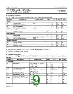
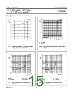
14.2 Output power
The output power versus supply voltage has been
measured on the output pins of one channel, and at
THD = 10%. The maximum output power is limited by the
maximum supply voltage of 18 V and the maximum
available output current: 4 A repetitive peak current.
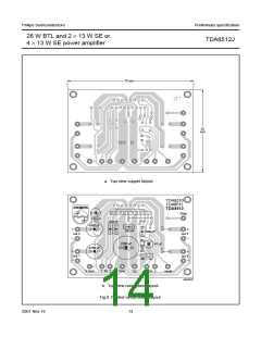
14.6 PCB layout and grounding
For high system performance level certain grounding
techniques are imperative. The input reference grounds
have to be tied with their respective source grounds, and
must have separate traces from the power ground traces;
this will separate the large (output) signal currents from
interfering with the small AC input signals. The
small-signal ground traces should be physically located as
far as possible from the power ground traces. Supply- and
output-traces should be as wide as practical for delivering
maximum output power. The PCB layout, which
accommodates the TDA8510, TDA8511, and TDA8512
products, is shown in Fig.8.
14.3 Power dissipation
The power dissipation graphs are given for one output
channel in SE, respectively BTL application. So for total
worst-case power dissipation the Pd of each channel must
be added up.
14.4 Supply Voltage Ripple Rejection (SVRR)
The SVRR is measured with an electrolytic capacitor of
100 µF on pin RR and at a bandwidth of 10 Hz to 80 kHz,
whereas the lowest frequencies can be lower than 10 Hz.
Proper supply bypassing is critical for low noise
performance and high power supply rejection. The
respective capacitor locations should be as close to the
device as possible, and grounded to the power ground. A
proper power supply decoupling also prevents oscillations.
2001 Nov 16
11

 NXP [ NXP ]