Philips Semiconductors
Preliminary specification
26 W BTL and 2 × 13 W SE or
4 × 13 W SE power amplifier
TDA8512J
7
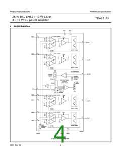
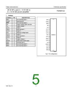
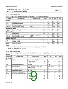
PINNING
SYMBOL
PIN
DESCRIPTION
non-inverting input 1
INV1
SGND
INV2
RR
1
2
INV1
1
2
3
4
5
6
7
8
9
signal ground
SGND
3
non-inverting input 2
supply voltage ripple rejection
supply voltage 1
output 1
INV2
RR
4
VP1
5
V
P1
OUT1
GND1
OUT2
REF
6
OUT1
GND1
OUT2
7
power ground 1
output 2
8
9
reference voltage input
output 3
OUT3
GND2
OUT4
VP2
10
11
12
13
14
15
16
17
REF
TDA8512J
power ground 2
output 4
OUT3 10
11
12
13
14
15
16
17
GND2
OUT4
supply voltage 2
mode select switch input
inverting input 3
non-inverting input 3
non-inverting input 4
MODE
INV3
INV3
INV4
V
P2
MODE
INV3
INV3
INV4
MGW427
Fig.2 Pin configuration.
2001 Nov 16
5

 NXP [ NXP ]