Philips Semiconductors
Preliminary specification
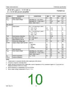
26 W BTL and 2 × 13 W SE or
4 × 13 W SE power amplifier
TDA8512J
8
FUNCTIONAL DESCRIPTION
8.2
Mode select
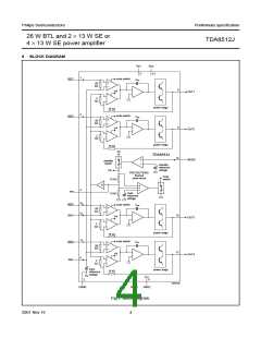
The TDA8512J contains four identical amplifiers and can
be used in the configurations:
For the 3 functional modes; standby, mute and operate,
the pin MODE can be driven by a 3-state logic output
stage: e.g. microcontroller with some extra components for
DC level shifting. (see Fig.10).
• Two SE channels (fixed gain 20 dB) and one BTL
channel (fixed gain 26 dB)
Standby mode will be activated by a applying a low
DC level between 0 and 2 V. The power consumption of
the device will be reduced to less than 1.5 mW. The input
and output pins are floating: high impedance condition.
• Four SE channels.
(RL depends on the application).
8.1
Mode select switch
Mute mode will be activated by a applying a DC level
between 3.3 and 6.4 V. The outputs of the amplifier will be
muted (no audio output); however, the amplifier is
DC biased and the DC level of the input and output pins
stays on half the supply voltage.
A special feature of the TDA8512J device is the mode
select switch (pin MODE), offering:
• Low standby current (<100 µA)
• Low switching current (low cost supply switch)
• Mute facility.
Operating mode is obtained at a DC level between 8.5 V
and VP.
To avoid switch-on plops, it is advised to keep the amplifier
in the mute mode for longer than 100 ms to allow charging
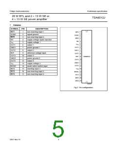
of the input capacitors at pins INV1, INV2, INV3, INV3
and INV4. This can be achieved by:
8.3
Built-in protection circuits
The device contains both a thermal protection, and a
short-circuit protection.
• Control via a microcontroller
Thermal protection:
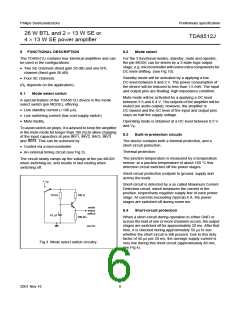
• An external timing circuit (see Fig.3).
The junction temperature is measured by a temperature
sensor; at a junction temperature of about 160 °C this
detection circuit switches off the power stages.
The circuit slowly ramps up the voltage at the pin MODE
when switching on, and results in fast muting when
switching off.
Short-circuit protection (outputs to ground, supply and
across the load):
V
P
handbook, halfpage
Short-circuit is detected by a so called Maximum Current
Detection circuit, which measures the current in the
positive, respectively negative supply line of each power
stage. At currents exceeding (typical) 6 A, the power
stages are switched off during some ms.
10 kΩ
47 µF
100 Ω
mode
select
switch
8.4
Short-circuit protection
100 kΩ
When a short-circuit during operation to either GND or
across the load of one or more channels occurs, the output
stages are switched off for approximately 20 ms. After that
time, it is checked during approximately 50 µs to see
whether the short-circuit is still present. Due to this duty
factor of 50 µs per 20 ms, the average supply current is
very low during this short-circuit (approximately 40 mA,
see Fig.4).
MGA708
Fig.3 Mode select switch circuitry.
2001 Nov 16
6

 NXP [ NXP ]