Philips Semiconductors
Preliminary specification
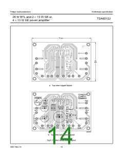
26 W BTL and 2 × 13 W SE or
4 × 13 W SE power amplifier
TDA8512J
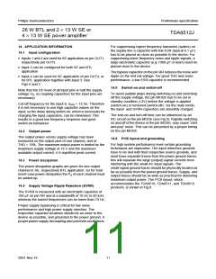
SYMBOL
Zi
PARAMETER
input impedance
noise output voltage
CONDITIONS
MIN.
25
TYP.
MAX. UNIT
30
38
kΩ
µV
µV
µV
Vn(o)
operating; Rs = 0 Ω; note 4
operating; Rs = 10 kΩ; note 4
mute; notes 4 and 5
−
−
−
70
−
100
60
200
−
SE channels
Po
output power
RL1 = 2 Ω (see Fig.7); note 1
THD = 0.5%
8.0
10.0
13.0
−
−
W
W
THD = 10%
11.0
R
L1 = 4 Ω (see Fig.7); note 1
THD = 0.5%
−
5.5
7.0
0.06
25
−
W
THD = 10%
−
−
W
THD
fro(l)
total harmonic distortion
low frequency roll-off
Po = 1 W
−
−
%
at −1 dB; note 2
at −1 dB
−
−
Hz
kHz
dB
fro(h)
Gv
high frequency roll-off
20
19
−
−
closed loop voltage gain
supply voltage ripple rejection
20
21
SVRR
note 3;
operating
mute
48
46
80
50
−
−
−
dB
dB
dB
kΩ
µV
µV
µV
dB
dB
−
−
standby
−
−
Zi
input impedance
60
50
70
50
60
−
75
−
Vn(o)
noise output voltage
operating; Rs = 0 Ω; note 4
operating; Rs = 10 kΩ; note 4
mute; notes 4 and 5
Rs = 10 kΩ
−
100
−
−
αcs
channel separation
channel unbalance
40
−
−
∆GV
1
Notes
1. Output power is measured directly at the output pins of the device.
2. Frequency response externally fixed.
3. Ripple rejection measured at the output with a source impedance of 0 Ω; maximum ripple of 2 V (p-p) and at a
frequency between 100 Hz to 10 kHz.
4. Noise measured in a bandwidth of 20 Hz to 20 kHz.
5. Noise output voltage independant of Rs (Vi = 0 V).
2001 Nov 16
10

 NXP [ NXP ]