Philips Semiconductors
Product specification
Multimedia bridge, high performance
Scaler and PCI circuit (SPCI)
SAA7146A
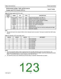
The I2C-bus interface is programmed through the transfer
control register (IICTRF) which is shown in Table 112.
A write to this register starts the transfer sequence where
up to 3 bytes are transferred: BYTE2, BYTE1 and BYTE0.
Any of these 3 bytes may be disabled or enabled for use
(as data byte or 7-bit address plus RW bit) in three I2C-bus
protocol functions:
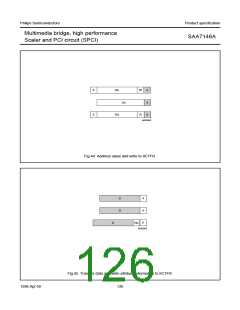
7.17 I2C-bus interface
7.17.1 GENERAL DESCRIPTION
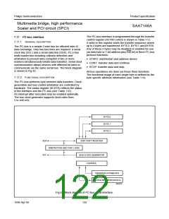
The I2C-bus is a simple 2-wire bus for efficient inter-IC
data exchange. Only two bus lines are required: a serial
clock line (SCL) and a serial data line (SDA). It’s a true
multi-master bus including collision detection and
arbitration to prevent data corruption if two or more
masters simultaneously initiate data transfers. Serial clock
synchronization allows devices with different bit rates to
communicate via the same serial bus. The block diagram
is shown in Fig.42.
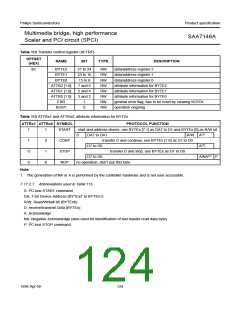
• START: start/restart and address device
• CONT: transfer data and continue
• STOP: transfer data and stop.
All bus operations are done via these three functions.
The functional usage of each single byte is defined by the
byte specific attribute information (see Table 113).
7.17.2 FUNCTIONAL DESCRIPTION
The I2C-bus performs byte oriented data transfers. Clock
generation and bus control arbitration are controlled by
hardware. The status register (IICSTA) reflects the status
of the interface and the I2C-bus (see Table 110).
An interrupt after execution may be enabled optionally.
The bus clock generator supports clock rates from
5 to 400 kHz.
handbook, full pagewidth
BYTE 0
BYTE 1
BYTE 2
SDA
SCL
8-BIT SHIFT REGISTER
ARBITRATION AND SYNC LOGIC
BUS CLOCK GENERATOR
CONTROL
TRANSFER ATTRIBUTES
STATUS REGISTER (IICSTA)
MGG278
Fig.42 Block diagram of I2C-bus serial interface.
1998 Apr 09
122

 NXP [ NXP ]