Philips Semiconductors
Product specification
Multimedia bridge, high performance
Scaler and PCI circuit (SPCI)
SAA7146A
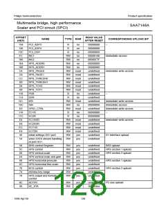
Table 112 Transfer control register (IICTRF)
OFFSET
(HEX)
NAME
BIT
TYPE
DESCRIPTION
8C
BYTE2
BYTE1
31 to 24
23 to 16
15 to 8
7 and 6
5 and 4
3 and 2
1
RW
RW
RW
RW
RW
RW
RW
RW
data/address register 2
data/address register 1
data/address register 0
BYTE0
ATTR2 [1:0]
ATTR1 [1:0]
ATTR0 [1:0]
ERR
attribute information for BYTE2
attribute information for BYTE1
attribute information for BYTE0
general error flag: has to be reset by clearing IICSTA
operation ongoing
BUSY
0
Table 113 ATTRx1 and ATTRx0; attribute information for BYTEx
ATTRx1 ATTRx0 SYMBOL
PROTOCOL FUNCTION
start and address device, use BYTEx [7:1] as DA7 to D1 and BYTEx [0] as R/W bit
DA7 to DA1
R/W A(1)
transfer D and continue, use BYTEx [7:0] as D7 to D0
1
1
0
0
1
0
1
0
START
CONT
STOP
NOP
S
D7 to D0
A(1)
transfer D and stop, use BYTEx as D7 to D0
D7 to D0
A/NA(1)
P
no operation, don’t use this byte
Note
1. The generation of NA or A is performed by the controller hardware and is not user accessible.
7.17.2.1 Abbreviations used in Table 113
S: I2C-bus START command
DA: 7-bit Device Address (BYTEx7 to BYTEx1)
R/W: Read/Write# bit (BYTEx0)
D: receive/transmit Data (BYTEx)
A: Acknowledge
NA: Negative Acknowledge (also used for identification of last master read data byte)
P: I2C-bus STOP command.
1998 Apr 09
124

 NXP [ NXP ]