Philips Semiconductors
Product specification
Multimedia bridge, high performance
Scaler and PCI circuit (SPCI)
SAA7146A
7.16.2 BASICS OF I2S-BUS SPECIFICATION
7.16 Audio interface
The I2S-bus transports digital audio (sound) signals
serially between ICs and consists of three signals:
7.16.1 GENERAL DESCRIPTION
The SAA7146A has two independent audio interface
circuits (A1 and A2) for serial input and output of digital
audio data streams. The audio interface circuits are based
on the I2S-bus standard but can be configured to several
data and timing formats (with respect to framing, bit clock
and synchronisation). LSB first (Sony) formats are not
supported. Up to 5 audio devices with separate serial data
lines and dedicated word select lines can be connected
directly. The interface also supports devices that share
one serial data line for multiple devices to transmit data in
different time slots. A time slot consists of one (serial) byte.
Each interface circuit supports up to 5 serial data lines and
related framing signals. A1 and A2 have the same internal
structure. They share the audio interface pins, i.e. the pins
can be accessed and utilized by one or the other audio
interface circuits at a time.
• A continuous bit clock BCLK (or SCK) with
(n × 8) multiple of the audio sample frequency
• A serial data wire SD, transporting the data in serial
bursts with MSB first
• A framing signal WS (Word Select) defining
(synchronizing) the start of a serial data burst.
WS and BCLK signals are provided by the master device.
The SAA7146A audio interfaces can be configured as
master or slave.
A data receiver must latch the data on SD line with the
rising edge of the bit clock BCLK. To satisfy the
requirements regarding set-up and hold times more easily
(and secure) it is recommended that the transmitter sends
its data on the falling edge. Set-up and hold times are
specified ‘parameterized’; i.e. as a percentage of the
actual bit clock. The serial data starts one clock cycle after
an edge of WS or synchronous to the edge. The word
(burst) length of transmitter and receiver may be different.
Missing LSBs are filled with zeros, excess LSBs are
truncated. There are other formats for transmitting serial
digital audio data between ICs which are slightly different
but still very similar to the I2S. The data set-up and hold
times or even the definition of an active clock edge may
vary. The word select or framing signal can be ‘in sync’
with the MSB of the data burst instead of one clock cycle
ahead. The Sony format is quite different, as it starts with
LSB first.
In order to support systems with asynchronous or mixed
audio sampling rates (e.g. 48 and 44.1 kHz raster, or
48 kHz 2 × 16-bit stereo and 8 kHz 8-bit mono), the two
audio interface circuits can run independently and even
asynchronously regarding bit clock rate, sampling rate and
framing (word select) signals. The two circuits can also be
combined into one synchronous interface sharing bit clock
and framing and sampling frequencies. Each audio
interface has two FIFOs (one for input and one for output),
and two associated DMA control circuits (one for master
read and one for master write), to exchange data with any
PCI address, e.g. main memory. The data structure and
signal flow control is time slot oriented and also supports
local feedback from input to output and from one timeslot
to another time slot. A set of time slots can be looped into
one ‘audio super frame’ containing up to 256 bits (32 time
slots). The signal flow is defined per time slot and
programmed by a time slot list.
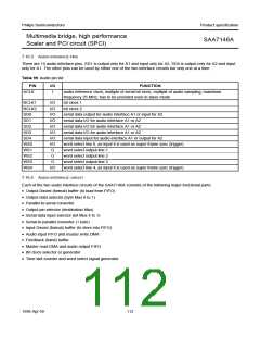
handbook, full pagewidth
WS
BCLK
ACLK
(reference clock)
MASTER
SLAVE
SD IN/OUT
MGG275
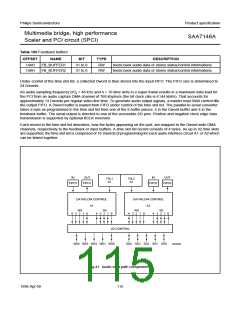
Fig.38 General application schematic of the audio interface.
1998 Apr 09
111

 NXP [ NXP ]