Philips Semiconductors
Product specification
Multimedia bridge, high performance
Scaler and PCI circuit (SPCI)
SAA7146A
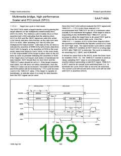
Larger TIMEOUT values would lead to wider read/write
pulses (pulse width = TIMEOUT + 1 [PCI clock cycles]).
Disabling the FAST mode would force 2 PCI clock cycles
Idle time between read/write strobes. It is not possible to
adjust the address phase timing. It is also assumed in this
figure that the RDY signal is not used (tied to HIGH level).
Use of the RDY signal is allowed in this mode and further
explained in the next example.
7.15.4.3 Transfer configuration
When using ‘dumb’ targets (unable to handshake) or ‘slow’
targets (unable to pull DTACK_RDY immediately), the
cycle length is adjusted by using a programmable cycle
timer. At TIMEOUT in Motorola mode the transfer control
gets into a defined state by finishing the cycle when a slave
is hanging or not able to handshake. In Intel mode the
transfer control waits for RDY = 1 after TIMEOUT, i.e. the
timer reflects the RDY reaction time of the target. In any
TIMEOUT case the Timer overflow Interrupt (TI) flag is set.
The timer starts at the falling edge of
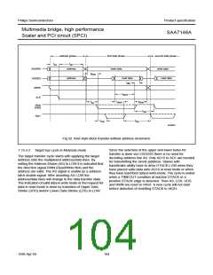
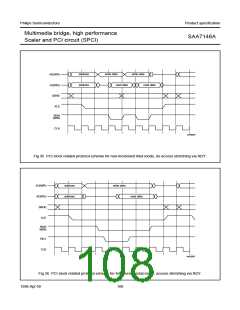
Figure 36 shows the incremental mode access. This mode
will produce an address phase prior to each data phase,
and as such has much lower bandwidth than the
non-incremental mode. In the example shown, the RDY
signal is also used, although that is not a requirement of
this mode. The overhead for this type of access is 2 PCI
cycles for address phase plus 2 PCI cycles for data
transfer phase plus 3 PCI cycles for write (4 PCI cycles for
read) Idle time between the data phase and the next
address phase. In the example shown, since RDY was
used with a TIMEOUT of 2, the resulting data phase was
4 PCI cycles, rather than the minimum of 2. In this
example the RDY de-asserts within the same PCI clock
cycle as RDN/WRN, which means RDY LOW is strobed by
the DEBI interface 1 PCI clock cycle after setting
RDN/WRN to LOW (parameter tmin = 1 PCI clock cycle).
Due to this a TIMEOUT = tmin + 1 = 2 (or greater) is
required for flexible access stretching, i.e. synchronizing
the RDY and stretching the access until RDY is released
to HIGH (see description of tmin in the timing parameters;
Table 93). In difference to the example without RDY
usage, increasing the value in TIMEOUT will NOT result in
wider read/write strobes, as long as the TIMEOUT value
does not exceed the RDY LOW phase by more than 1 PCI
clock cycle. Enabling or disabling the FAST mode has no
effect in incremental mode.
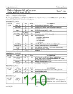
UDS_WRN/LDS_RDN. For initiating a transfer the target
address must be specified (16-bit, pointing to the first byte
to transfer), the transfer direction (WRITE_n) and the
BLOCKLENGTH that indicates how many bytes have to
be transferred. For block transfer a 32-bit DMA start
address (PCI) has to be specified in the DEBI_AD register.
When the BLOCKLENGTH is 1 to 4 bytes the data is
immediately transferred to/from the DEBI_AD register.
Immediate transfer crossing a Dword boundary is not
allowed. Such illegal transfer trials are reported by the
Format Error bit (FE) in the status register. Immediate
transfer starts with the least significant byte/word of the
DEBI_AD register.
The following figures illustrate the protocol of the DEBI bus
for Intel mode transfers. These figures contain no formal
timing specification (see Table 93 for timing) but rather are
intended to help in understanding the operation of the
DEBI interface. The DEBI bus protocol operates in step
with the PCI clock, so it is shown for reference at the
bottom of these diagrams. At slower PCI clock rates, the
DEBI transaction time is proportionally increased. It is not
necessary to connect a PCI clock to the DEBI target
system, since DEBI does not expect target read data or
target driven handshake signals to be synchronous to PCI
clock.
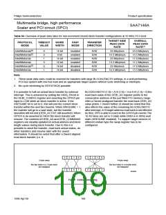
It should be noted that the minimum timing illustrated by
these diagrams is not the sustainable data rate by the
SAA7146A through the DEBI interface. PCI-bus latencies,
FIFO fullness, target behaviour and other factors will affect
the sustained data rate. For illustration purposes Table 94
provides indication of peak data rates in various DEBI
configurations.
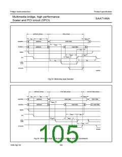
Figure 35 shows the non-incremental mode access in the
fastest possible configuration (TIMEOUT = 0; FAST = 1).
The overhead for this type of access is 2 PCI clock cycles
for address phase plus 2 PCI clock cycles for each data
phase. In this mode, the blocks are easily identified by the
falling edge of ALE indicating a new target address can be
latched.
1998 Apr 09
107

 NXP [ NXP ]