Philips Semiconductors
Product specification
Multimedia bridge, high performance
Scaler and PCI circuit (SPCI)
SAA7146A
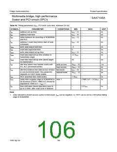
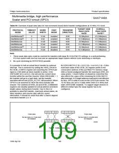
Table 94 Overview of peak data rates for non-increment (burst) block transfer configurations at 33 MHz PCI clock
TARGET SIDE
PEAK DATA
RATE
OVERALL
PEAK DATA
RATE(1)
PROTOCOL
MODE
TIMEOUT
VALUE
WORD
WIDTH
FAST
MODE
TRANSFER
DIRECTION
Intel/Motorola(2)
Intel/Motorola(2)
Intel/Motorola
Intel/Motorola
Intel/Motorola(2)
Intel/Motorola
0
0
1
3
0
1
16 bit
8 bit
enabled
enabled
enabled
enabled
disabled
disabled
R/W
R/W
R/W
R/W
R/W
R/W
33 Mbytes/s
16.5 Mbytes/s
22 Mbytes/s
13.2 Mbytes/s
22 Mbytes/s
16.5 Mbytes/s
23.0 Mbytes/s
13.5 Mbytes/s
17.0 Mbytes/s
11.2 Mbytes/s
17.0 Mbytes/s
13.5 Mbytes/s
16 bit
16 bit
16 bit
16 bit
Note
1. These peak data rates could be reached for transfers with large BLOCKLENGTH settings, in a well performing
PCI-bus system with low bus load and an appropriate target system without cycle stretching or interrupts.
2. No cycle stretching by RDY/DTACK possible.
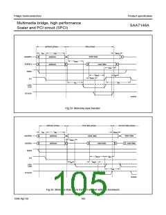
It is possible to halt an actual block transfer by external
interrupt. This is achieved by setting the XIRQ_EN bit in
the DEBI_CONFIG register and asserting the GPIO3 pin
input to LOW while an block transfer is active. If the
XRESUME bit is set to 0, this will end the current block
transfer within the next two Dwords. When XRESUME = 1
the transfer will go to a wait state, but the transfer
operation will not end (DEBI_ACTIVE still asserted). When
GPIO3 is de-asserted to HIGH the block transfer will
resume. The contents of DEBI_AD and DEBI_COMMAND
registers are steadily updated on actual address and block
length values during block transfer. Due to this it is
possible to abort the transfer, read back actual status, do
other transfers and resume later with the saved
BLOCKLENGTH [1:0] + A16 [1:0] = 4 or A16 [1:0] = 0) the
read back value of the DEBI_AD register points to the
consecutive address of the just filled PCI memory range.
After a Dword unaligned transfer the read back DEBI_AD
value points 1 Dword further (it should be noted that this
also effects the value of the remaining BLOCKLENGTH
after interrupt; A16 target address read back is not effected
by this). RPS is able to react on the GPIO3 pin events.The
16 AD lines are set to 3-state while DEBI is in XIRQ wait
state (XRESUME enabled). To support target devices of
different endian type the swap register has to be
configured.
information. It should be noted that after a Dword aligned
read block transfer (i.e. if
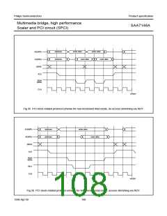
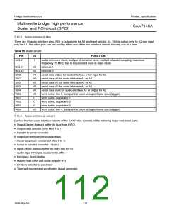
handbook, full pagewidth
3
2
2
3
1
0
0
1
3
0
2
1
1
2
0
3
2-byte swap
4-byte swap
the two bytes in a 2-byte word
are swapped
the four bytes in a double word
are swapped
MHB069
Fig.37 Endian swapping.
1998 Apr 09
109

 NXP [ NXP ]