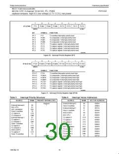
Philips Semiconductors
Preliminary specification
80C51 8-bit microcontroller
8K/256 OTP, 8 channel 10 bit A/D, I2C, PWM,
capture/compare, high I/O, low voltage (2.7V–5.5V), low power
P87C552
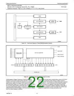
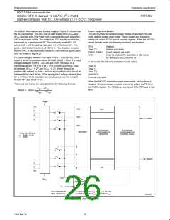
10-Bit ADC Resolution and Analog Supply: Figure 23 shows how
the ADC is realized. The ADC has its own supply pins (AV and
Power Reduction Modes
The 8XC552 has two reduced power modes of operation: the idle
mode and the power-down mode. These modes are entered by
setting bits in the PCON special function register. When the 8XC552
enters the idle mode, the following functions are disabled:
DD
AV ) and two pins (Vref+ and Vref–) connected to each end of the
SS
DAC’s resistance-ladder. The ladder has 1023 equally spaced taps,
separated by a resistance of “R”. The first tap is located 0.5 x R
above Vref–, and the last tap is located 1.5 x R below Vref+. This
gives a total ladder resistance of 1024 x R. This structure ensures
that the DAC is monotonic and results in a symmetrical quantization
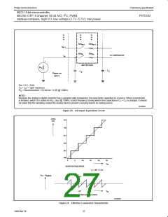
error as shown in Figure 25.
CPU
(halted)
Timer T2
PWM0, PWM1
ADC
(halted and reset)
(reset; outputs are high)
(may be enabled for operation in Idle mode
by setting bit AIDC (AUXR1.6) ).
For input voltages between Vref– and (Vref–) + 1/2 LSB, the 10-bit
result of an A/D conversion will be 00 0000 0000B = 000H. For input
voltages between (Vref+) – 3/2 LSB and Vref+, the result of a
conversion will be 11 1111 1111B = 3FFH. AVref+ and AVref– may
be between AV + 0.2V and AV – 0.2V. AVref+ should be
In idle mode, the following functions remain active:
Timer 0
Timer 1
DD
SS
positive with respect to AVref–, and the input voltage (Vin) should be
between AVref+ and AVref–. If the analog input voltage range is from
2V to 4V, then 10-bit resolution can be obtained over this range if
AVref+ = 4V and AVref– = 2V.
Timer T3
SIO0 SIO1
External interrupts
When the 8XC552 enters the power-down mode, the oscillator is
stopped. The power-down mode is entered by setting the PD bit in
the PCON register. The PD bit can only be set if the EW input is tied
HIGH.
The result can always be calculated from the following formula:
V
IN * AVref*
Result + 1024
AVref) * AVref*
AV
ref+
R/2
1023
1022
MSB
R
R
R
START
1021
SUCCESSIVE
APPROXIMATION
REGISTER
SUCCESSIVE
APPROXIMATION
CONTROL LOGIC
DECODER
TOTAL RESISTANCE
=
=
1023R + 2 x R/
1024R
3
2
READY
R
R
1
0
LSB
R/2
V
–
ref
AV
ref–
COMPARATOR
+
V
in
Value 0000 0000 00
Value 1111 1111 11
is output for voltages V
is output for voltages (V
ref+
to (V
+ 1/2 LSB)
ref–
ref–
– 3/2 LSB) to V
ref+
SU00961
Figure 23. ADC Realization
26
1999 Mar 30

 NXP [ NXP ]