Philips Semiconductors
Preliminary specification
80C51 8-bit microcontroller
8K/256 OTP, 8 channel 10 bit A/D, I2C, PWM,
capture/compare, high I/O, low voltage (2.7V–5.5V), low power
P87C552
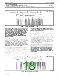
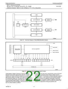
PWM0
OUTPUT
BUFFER
8-BIT COMPARATOR
PWM0
f
OSC
1/2
PRESCALER
PWMP
8-BIT COUNTER
OUTPUT
BUFFER
PWM1
8-BIT COMPARATOR
PWM1
SU00956
Figure 18. Functional Diagram of Pulse Width Modulated Outputs
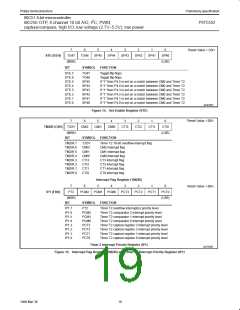
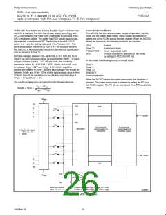
STADC
ADC0
ADC1
+
–
ANALOG REF.
ADC2
ADC3
ADC4
ADC5
ANALOG INPUT
MULTIPLEXER
10-BIT A/D CONVERTER
ANALOG SUPPLY
ANALOG GROUND
ADC6
ADC7
ADCON
ADCH
0
1
2
3
4
5
6
7
0
1
2
3
4
5
6
7
INTERNAL BUS
SU00957
Figure 19. Functional Diagram of Analog Input Circuitry
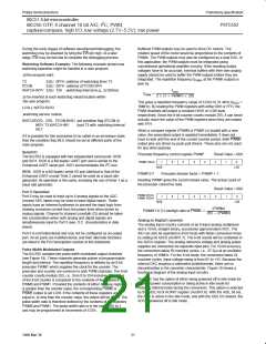
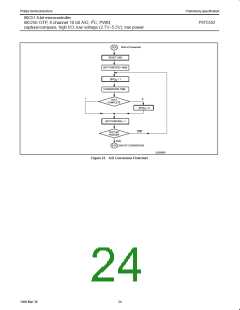
10-Bit Analog-to-Digital Conversion: Figure 20 shows the
elements of a successive approximation (SA) ADC. The ADC
contains a DAC which converts the contents of a successive
approximation register to a voltage (VDAC) which is compared to
the analog input voltage (Vin). The output of the comparator is fed to
the successive approximation control logic which controls the
successive approximation register. A conversion is initiated by
setting ADCS in the ADCON register. ADCS can be set by software
only or by either hardware or software.
The software only start mode is selected when control bit ADCON.5
(ADEX) = 0. A conversion is then started by setting control bit
ADCON.3 (ADCS). The hardware or software start mode is selected
when ADCON.5 = 1, and a conversion may be started by setting
ADCON.3 as above or by applying a rising edge to external pin
STADC. When a conversion is started by applying a rising edge, a
low level must be applied to STADC for at least one machine cycle
followed by a high level for at least one machine cycle.
22
1999 Mar 30

 NXP [ NXP ]