Philips Semiconductors
Preliminary specification
80C51 8-bit microcontroller
8K/256 OTP, 8 channel 10 bit A/D, I2C, PWM,
capture/compare, high I/O, low voltage (2.7V–5.5V), low power
P87C552
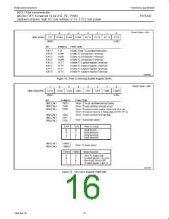
Reset Value = 00H
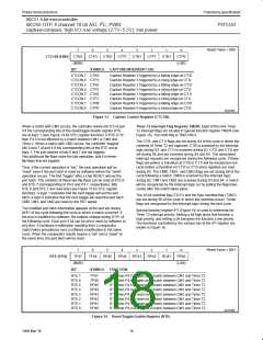
7
CTCON (EBH) CTN3
(MSB)
6
5
4
3
2
1
0
CTP3
CTN2
CTP2
CTN1
CTP1
CTN1
CTP0
(LSB)
BIT
SYMBOL CAPTURE/INTERRUPT ON:
CTCON.7 CTN3
Capture Register 3 triggered by a falling edge on CT3I
Capture Register 3 triggered by a rising edge on CT3I
Capture Register 2 triggered by a falling edge on CT2I
Capture Register 2 triggered by a rising edge on CT2I
Capture Register 1 triggered by a falling edge on CT1I
Capture Register 1 triggered by a rising edge on CT1I
Capture Register 0 triggered by a falling edge on CT0I
Capture Register 0 triggered by a rising edge on CT0I
CTCON.6 CTP3
CTCON.5 CTN2
CTCON.4 CTP2
CTCON.3 CTN1
CTCON.2 CTP1
CTCON.1 CTN0
CTCON.0 CTP0
SU01085
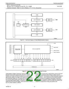
Figure 13. Capture Control Register (CTCON)
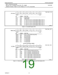
When a match with CM1 occurs, the controller resets bits 0-5 of port
4 if the corresponding bits of the reset/toggle enable register RTE
are at logic 1 (see Figure 14 for RTE register function). If RTE is “0”,
then P4.n is not affected by a match between CM1 or CM2 and
Timer 2. When a match with CM2 occurs, the controller “toggles”
bits 6 and 7 of port 4 if the corresponding bits of the RTE are at
logic 1. The port latches of bits 6 and 7 are not toggled.
Two additional flip-flops store the last operation, and it is these
flip-flops that are toggled.
Timer T2 Interrupt Flag Register TM2IR: Eight of the nine Timer
T2 interrupt flags are located in special function register TM2IR (see
Figure 16). The ninth flag is TM2CON.4.
The CT0I and CT1I flags are set during S4 of the cycle in which the
contents of Timer T2 are captured. CT0I is scanned by the interrupt
logic during S2, and CT1I is scanned during S3. CT2I and CT3I are
set during S6 and are scanned during S4 and S5. The associated
interrupt requests are recognized during the following cycle. If these
flags are polled, a transition at CT0I or CT1I will be recognized one
cycle before a transition on CT2I or CT3I since registers are read
during S5. The CMI0, CMI1, and CMI2 flags are set during S6 of the
cycle following a match. CMI0 is scanned by the interrupt logic
during S2; CMI1 and CMI2 are scanned during S3 and S4. A match
will be recognized by the interrupt logic (or by polling the flags) two
cycles after the match takes place.
Thus, if the current operation is “set,” the next operation will be
“reset” even if the port latch is reset by software before the “reset”
operation occurs. The first “toggle” after a chip RESET will set the
port latch. The contents of these two flip-flops can be read at STE.6
and STE.7 (corresponding to P4.6 and P4.7, respectively). Bits
STE.6 and STE.7 are read only (see Figure 15 for STE register
function). A logic 1 indicates that the next toggle will set the port
latch; a logic 0 indicates that the next toggle will reset the port latch.
CM0, CM1, and CM2 are reset by the RST signal.
The 16-bit overflow flag (T2OV) and the byte overflow flag (T2BO)
are set during S6 of the cycle in which the overflow occurs. These
flags are recognized by the interrupt logic during the next cycle.
The modified port latch information appears at the port pin during
S5P1 of the cycle following the cycle in which a match occurred. If
the port is modified by software, the outputs change during S1P1 of
the following cycle. Each port 4 bit can be set or reset by software at
any time. A hardware modification resulting from a comparator
match takes precedence over a software modification in the same
cycle. When the comparator results require a “set” and a “reset” at
the same time, the port latch will be reset.
Special function register IP1 (Figure 16) is used to determine the
Timer T2 interrupt priority. Setting a bit high gives that function a
high priority, and setting a bit low gives the function a low priority.
The functions controlled by the various bits of the IP1 register are
shown in Figure 16.
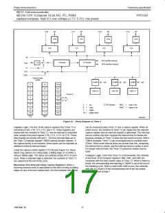
Reset Value = 00H
7
6
5
4
3
2
1
0
RTE (EFH)
TP47
(MSB)
TP46
RP45
RP44
RP43
RP42
RO41
RP40
(LSB)
BIT
SYMBOL FUNCTION
RTE.7
RTE.6
RTE.5
RTE.4
RTE.3
RTE.2
RTE.1
RTE.0
TP47
TP46
RP45
RP44
RP43
RP42
RP41
RP40
If “1” then P4.7 toggles on a match between CM1 and Timer T2
If “1” then P4.6 toggles on a match between CM1 and Timer T2
If “1” then P4.5 is reset on a match between CM1 and Timer T2
If “1” then P4.4 is reset on a match between CM1 and Timer T2
If “1” then P4.3 is reset on a match between CM1 and Timer T2
If “1” then P4.2 is reset on a match between CM1 and Timer T2
If “1” then P4.1 is reset on a match between CM1 and Timer T2
If “1” then P4.0 is reset on a match between CM1 and Timer T2
SU01086
Figure 14. Reset/Toggle Enable Register (RTE)
18
1999 Mar 30

 NXP [ NXP ]