Philips Semiconductors
Preliminary specification
80C51 8-bit microcontroller
8K/256 OTP, 8 channel 10 bit A/D, I2C, PWM,
capture/compare, high I/O, low voltage (2.7V–5.5V), low power
P87C552
During the early stages of software development/debugging, the
watchdog may be disabled by tying the EW pin high. At a later
stage, EW may be tied low to complete the debugging process.
Buffered PWM outputs may be used to drive DC motors. The
rotation speed of the motor would be proportional to the contents of
PWMn. The PWM outputs may also be configured as a dual DAC. In
this application, the PWM outputs must be integrated using
conventional operational amplifier circuitry. If the resulting output
voltages have to be accurate, external buffers with their own analog
supply should be used to buffer the PWM outputs before they are
Watchdog Software Example: The following example shows how
watchdog operation might be handled in a user program.
;at the program start:
integrated. The repetition frequency f
give by:
, at the PWMn outputs is
PWM
T3
PCON
EQU 0FFH ;address of watchdog timer T3
EQU 087H ;address of PCON SFR
WATCH-INTV EQU 156 ;watchdog interval (e.g., 2x100ms)
fOSC
fPWM
+
2 (1 ) PWMP) 255
;to be inserted at each watchdog reload location within
;the user program:
This gives a repetition frequency range of 123Hz to 31.4kHz (f
=
OSC
16MHz). By loading the PWM registers with either 00H or FFH, the
PWM channels will output a constant HIGH or LOW level,
respectively. Since the 8-bit counter counts modulo 255, it can never
actually reach the value of the PWM registers when they are loaded
with FFH.
LCALL WATCHDOG
;watchdog service routine:
WATCHDOG: ORL PCON,#10H ;set condition flag (PCON.4)
MOV T3,WATCH-INV
RET
;load T3 with watchdog interval
When a compare register (PWM0 or PWM1) is loaded with a new
value, the associated output is updated immediately. It does not
have to wait until the end of the current counter period. Both PWMn
output pins are driven by push-pull drivers. These pins are not used
for any other purpose.
If it is possible for this subroutine to be called in an erroneous state,
then the condition flag WLE should be set at different parts of the
main program.
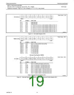
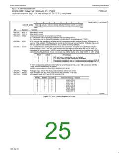
Serial I/O
Prescaler frequency control register PWMP
Reset Value = 00H
The 8xC552 is equipped with two independent serial ports: SIO0
and SIO1. SIO0 is a full duplex UART port and is similar to the
Enhanced UART serial port. SIO1 accommodates the I C bus.
PWMP (FEH)
7
6
5
4
3
2
1
0
2
MSB
LSB
SIO0: SIO0 is a full duplex serial I/O port identical to that of the
Enhanced UART except Time 2 cannot be used as a baud rate
generator. Its operation is the same, including the use of timer 1 as a
baud rate generator.
PWMP.0-7
Prescaler division factor = PWMP + 1.
Reading PWMP gives the current reload value. The actual count of
the prescaler cannot be read.
Reset Value = 00H
Port 5 Operation
PWM0 (FCH)
PWM1 (FDH)
Port 5 may be used to input up to 8 analog signals to the ADC.
Unused ADC inputs may be used to input digital inputs. These
inputs have an inherent hysteresis to prevent the input logic from
drawing excessive current from the power lines when driven by
analog signals. Channel to channel crosstalk (Ct) should be taken
into consideration when both analog and digital signals are
simultaneously input to Port 5 (see, D.C. characteristics in data
sheet).
7
6
5
4
3
2
1
0
MSB
LSB
(PWMn)
255 * (PWMn)
PWM0/1.0-7} Low/high ratio of PWMn +
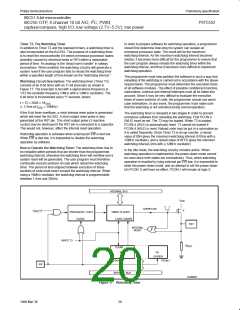
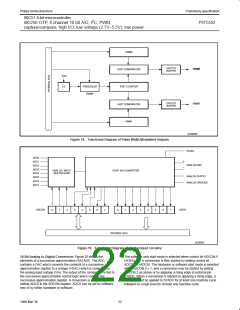
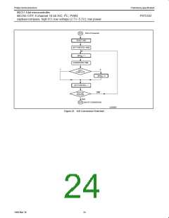
Analog-to-Digital Converter
The analog input circuitry consists of an 8-input analog multiplexer
and a 10-bit, straight binary, successive approximation ADC. The
A/D can also be operated in 8-bit mode with faster conversion times
by setting bit ADC8 (AUXR1.7). The 8-bit results will be contained in
the ADCH register. The analog reference voltage and analog power
supplies are connected via separate input pins. For 10-bit accuracy,
the conversion takes 50 machine cycles, i.e., 37.5µs at an oscillator
frequency of 16MHz. For the 8-bit mode, the conversion takes 24
machine cycles. Input voltage swing is from 0V to +5V. Because the
internal DAC employs a ratiometric potentiometer, there are no
discontinuities in the converter characteristic. Figure 19 shows a
functional diagram of the analog input circuitry.
Port 5 is not bidirectional and may not be configured as an output
port. All six ports are multifunctional, and their alternate functions
are listed in the Pin Descriptions section of this datasheet.
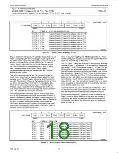
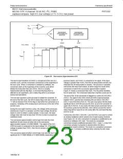
Pulse Width Modulated Outputs
The 8xC552 contains two pulse width modulated output channels
(see Figure 18). These channels generate pulses of programmable
length and interval. The repetition frequency is defined by an 8-bit
prescaler PWMP, which supplies the clock for the counter. The
prescaler and counter are common to both PWM channels. The 8-bit
counter counts modulo 255, i.e., from 0 to 254 inclusive. The value
of the 8-bit counter is compared to the contents of two registers:
PWM0 and PWM1. Provided the contents of either of these registers
is greater than the counter value, the corresponding PWM0 or
PWM1 output is set LOW. If the contents of these registers are
equal to, or less than the counter value, the output will be HIGH. The
pulse-width-ratio is therefore defined by the contents of the registers
PWM0 and PWM1. The pulse-width-ratio is in the range of 0 to 1
and may be programmed in increments of 1/255.
The ADC has the option of either being powered off in idle mode for
reduced power consumption or being active in idle mode for
reducing internal noise during the conversion. This option is selected
by the AIDL bit of AUXR1 register (AUXR1.6). With the AIDL bit set,
the ADC is active in the idle mode, and with the AIDL bit cleared, the
ADC is powered off in idle mode.
21
1999 Mar 30

 NXP [ NXP ]