Philips Semiconductors
PCA82C250 / 251 CAN Transceiver
Application Note
AN96116
uC
CAN - Contoller
CTX1CTX0 CRX0 CRX1 Px,y
/ TX1 / TX0 / RX0 / RX1
e.g. PCx82C200
either connection to an output port pin,
if standby mode shall be possible
or
connection to ground
0V
R
ext
TxD RxD
VREF
Rs
+5V
V
PCA 82C250/251
CAN Transceiver
CC
100n
0V
GND
CANH CANL
JK512151.GWM
ISO 11898 Standard
CAN Bus Line
CAN_H
CAN_L
124
124
Programming of the Output Control Register (example)
Output Control TX0 push-pull, dominant = low e.g. 1A
hex
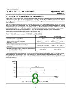
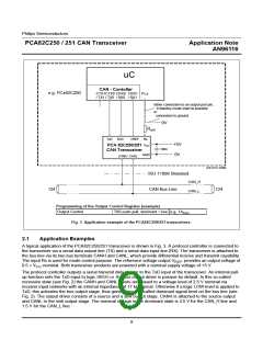
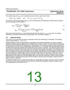
Fig. 3 Application example of the PCA82C250/251 transceivers
2.1
Application Examples
A typical application of the PCA82C250/251 transceiver is shown in Fig. 3. A protocol controller is connected to
the transceiver via a serial data output line (TX) and a serial data input line (RX). The transceiver is attached to
the bus line via its two bus terminals CANH and CANL, which provide differential receive and transmit capability.
The input Rs is used for mode control purpose. The reference voltage output V
provides an output voltage of
REF
0.5 × V
nominal. Both transceiver products are powered with a nominal supply voltage of +5 V.
CC
The protocol controller outputs a serial transmit data stream to the TxD input of the transceiver. An internal pull-
up function sets the TxD input to logic HIGH i.e. the bus output driver is passive by default. In this so-called
recessive state (see Fig. 2) the CANH and CANL inputs are biased to a voltage level of 2.5 V nominal via
receiver input networks with an internal impedance of 17 kΩ typical. Otherwise if a logic LOW-level is applied to
TxD, this activates the bus output stage, thus generating a so-called dominant signal level on the bus line (see
Fig. 2). The output driver consists of a source and a sink output stage. CANH is attached to the source output
and CANL to the sink output stage. The nominal voltage in the dominant state is 3.5 V for the CAN_H line and
1.5 V for the CAN_L line.
9

 NXP [ NXP ]