Philips Semiconductors
PCA82C250 / 251 CAN Transceiver
Application Note
AN96116
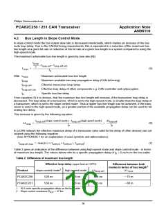
The suitable range for R
can be calculated using the limits for slope control mode
ext
10 µA < -I < 200 µA
and
0.4 × V
< V < 0.6 × V
.
CC
Rs
CC
Rs
The minimum and maximum values for R
tion of the symbols see APPENDIX 1).
can be calculated with the following two relations (for the explana-
ext
0.6V
0.6V
CC.max
CC.max
R
> ------------------------------ = ------------------------------
(1)
(2)
ext
I
200µA
Rs.max
0.4V
– V
0.4V
– V
CC.min OL.max
CC.min
OL.max
-----------------------------------------------------------
R
<
=
---------------------------------------------------------
ext
I
10µA
Rs.min
If the slope control resistor R
is connected to ground, then the value V
is zero volts. The relation
OL.max
ext
between the Rs output current and the bus signal slew rate is discussed in chapter 4.1.
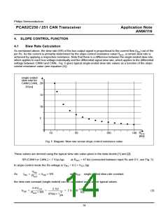
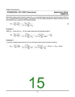
3.3
Stand-by Mode
This mode is to be used when the power consumption needs to be minimized e.g. temporarily. The stand-by
mode is selected with V > 0.75 × V
.
CC
Rs
Using the stand-by mode, the system power consumption can be reduced drastically. This mode is primarily
intended for battery powered applications for example when a vehicle is parked. To enter stand-by mode a logic
HIGH-level has to be applied to the transceiver´s control input Rs. This can be done either by direct connection of
an output port pin to Rs or via any suitable slope control resistor R . In stand-by mode the transmitter function
ext
and the receiver input bias network are switched off to reduce power consumption. The reference voltage output
and a basic receive function will remain active and work with very low power consumption. This allows to reacti-
vate the system via the bus line by transmission of a message. Upon detection of a dominant bus condition of at
least 3 µs length, the transceiver will provide a wake-up interrupt signal to the protocol controller via its RxD out-
put. Upon detection of a falling edge on RxD the controller should set the Rs pin to logic LOW-level in order to
switch the transceiver back to normal transmission mode. As the receiver is slower in stand-by mode, it essen-
tially depends on the delay time of the logic (falling edge on Rs) when the transceiver is back to normal reception
speed. At high bus speeds the transceiver may not be able to correctly receive messages in stand-by mode i.e.
while the Rs pin is still HIGH.
An alternative application is to connect the Rs input to an active-high reset signal. This can be done for example
with view to the case of the transceiver and the protocol controller being supplied by different supply sources,
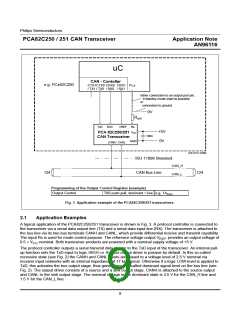
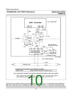
e.g. if optocouplers are used (see Fig. 4).
13

 NXP [ NXP ]