Philips Semiconductors
PCA82C250 / 251 CAN Transceiver
Application Note
AN96116
5. MAXIMUM BUS LINE LENGTH
The maximum achievable bus line length in a CAN bus network is determined essentially by the following physi-
cal effects:
1. The loop delays of the connected bus nodes (CAN controller, transceiver etc.) and the delay of the bus line
2. The differences in bit time quantum length due to the relative oscillator tolerance between nodes
3. The signal amplitude drop due to the series resistance of the bus cable and the input resistance of bus
nodes
The effect 3. is discussed below.
The effects 1. and 2. are not discussed in this document (please refer e.g. to [4]). However as a rule of thumb the
following bus line length can be achieved with the PCA82C250 and PCA82C251 in high-speed mode and with
CAN bit timing parameters being optimized for maximum propagation delay:
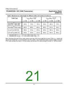
Table 3 Bit Rate / Bus Length Relation
Bit Rate (kbit/s)
Bus Length (m)
1000
500
250
125
62.5
30
100
250
500
1000
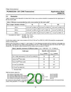
5.1
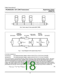
Impact of the Bus Cable Resistance
The ISO 11898 Standard [3] assumes the network wiring topology to be close to a single line structure in order to
minimize reflection effects on the bus line (Fig. 6).
At static conditions the differential input voltage at a bus node is determined by the current flowing through the
differential input resistance of that node. In case of a dominant bit the output transistors of the transmitting node
are switched on, causing a current flow, whereas the transistors are switched off for a recessive bit.
Thus the generated differential voltage at the input of a node (V
) depends on (see Fig. 7)
diff.in
• The differential output voltage of the transmitting nodes (V
)
diff.out
• The resistance of the bus cable (R = ρ × L) with
W
ρ = specific resistance per length unit and
L = length of the bus line
• The differential input resistance of receiving nodes (R
)
diff
The worst case situation is given for one transmitting node at one end of the bus wire and a receiving node at the
other end.
For this case the differential input voltage at the receiving node is calculated using Fig. 7 (see APPENDIX 2).
V
diff.out
V
= ------------------------------------------------------------
(8)
diff.in
1
n – 1
1 + 2R
×
+
------ -----------
W
R
R
T
diff
17

 NXP [ NXP ]