ISP1160
Embedded USB Host Controller
Philips Semiconductors
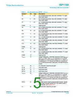
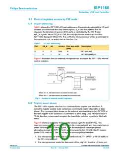
Table 2:
Pin description for LQFP64…continued
Symbol[1]
Pin
48
49
50
51
52
Type
-
Description
n.c.
no connection; leave this pin open
n.c.
-
no connection; leave this pin open
H_DM1
H_DP1
H_DM2
AI/O
AI/O
AI/O
USB D− data line for HC downstream port 1
USB D+ data line for HC downstream port 1
USB D− data line for HC downstream port 2; when not in
use, this pin must be left open
H_DP2
53
AI/O
USB D+ data line for HC downstream port 2; when not in
use, this pin must be left open
H_OC1_N
H_OC2_N
VCC
54
55
56
I
I
-
overcurrent sensing input for HC downstream port 1
overcurrent sensing input for HC downstream port 2
digital power supply input (3.0 V to 3.6 V or
4.75 V to 5.25 V). This pin supplies the internal 3.3 V
regulator input. When connected to 5 V, the internal
regulator will output 3.3 V to pins VREG(3V3), VHOLD1 and
VHOLD2. When connected to 3.3 V, it will bypass the internal
regulator.
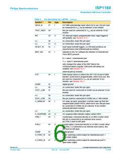
AGND
57
58
-
-
analog ground
VREG(3V3)
internal 3.3 V regulator output; when pin VCC is connected
to 5 V, this pin outputs 3.3 V. When pin VCC is connected to
3.3 V, connect this pin to 3.3 V.
A0
59
60
I
I
address input; selects command (A0 = 1) or data (A0 = 0)
LOW_PW
if low-current consumption (range of µs) is needed during
suspend, connect this pin to address A1; otherwise,
connect to DGND
n.c.
61
62
63
-
no connection; leave this pin open
digital ground
DGND
D0
-
I/O
bit 0 of bidirectional data; slew-rate controlled; TTL input;
three-state output
D1
64
I/O
bit 1 of bidirectional data; slew-rate controlled; TTL input;
three-state output
[1] Symbol names ending with underscore N (for example, NAME_N) represent active LOW signals.
9397 750 11371
© Koninklijke Philips Electronics N.V. 2003. All rights reserved.
Product data
Rev. 04 — 04 July 2003
7 of 88

 NXP [ NXP ]