xxxx xxxxxxxxxxxxxxxxxxxxxxxxxxxxxx x xxxxxxxxxxxxxx xxxxxxxxxx xxx xxxxxx xxxxxxxxxxxxxxxxxxxxxxx xxxxxxxxxxxxxxxxxxxxxx
xxxxx xxxxxx xx xxxxxxxxxxxxxxxxxxxxxxxxxxxxx xxxxxxxxxxxxxxxxxxxxxx xxxxxxxxxxx xxxxxxx xxxxxxxxxxxxxxxxxxx
xxxxxxxxxxxxxxxx xxxxxxxxxxxxxx xxxxxx xx xxxxxxxxxxxxxxxxxxxxxxxxxxxxxxxx xxxxxxxxxxxxxxxxxxxxxxxx xxxxxxx
xxxxxxxxxxxxxxxxxxxxxxxxxxxxxxxxxxxxxxxxxxxxxx xxxxxxxxxxx xxxxx x x
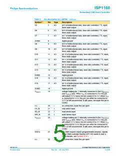
40
H_WAKEUP
46
47
54
55
42
33
H_PSW1_N
H_PSW2_N
H_OC1_N
H_OC2_N
H_SUSPEND
NDP_SEL
POWER
SWITCHING
ATL RAM
ITL0
ITL1
OVERCURRENT
DETECTION
(PING RAM) (PONG RAM)
2 to 7,
9 to 14,
16, 17,
63, 64
16
ISP1160
D0 to D15
22
21
23
59
27
34
25
29
RD_N
CS_N
50
51
52
53
H_DM1
USB
TRANSCEIVER
MICROPROCESSOR
BUS INTERFACE
WR_N
A0
DACK_N
USB bus
downstream
ports
H_DP1
H_DM2
HOST CONTROLLER
USB
TRANSCEIVER
H_DP2
EOT
DREQ
INT
4×
15 kΩ
32
56
RESET_N
internal
reset
POWER-ON
RESET
CLOCK
RECOVERY
PLL
GND
3.3 V
58
internal
supply
VOLTAGE
REGULATOR
V
CC
CLOCK
RECOVERY
20, 26, 30, 31, 36,
38, 41, 48, 49, 61
1, 8, 15, 18,
35, 45, 62
57
V
24
19
44
43
004aaa059
XTAL2
XTAL1
7
10
n.c.
REG(3V3)
V
6 MHz
V
DGND
AGND
1
HOLD
2
HOLD
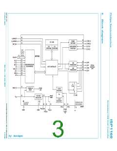
Fig 1. Block diagram.

 NXP [ NXP ]