ISP1160
Embedded USB Host Controller
Philips Semiconductors
16-bit register access cycle
write command
(16 bits)
read/write data
(16 bits)
t
MGT937
Fig 6. 16-bit register access cycle.
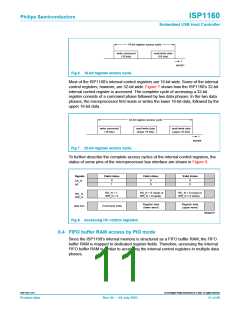
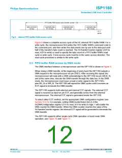
Most of the ISP1160’s internal control registers are 16-bit wide. Some of the internal
control registers, however, are 32-bit wide. Figure 7 shows how the ISP1160’s 32-bit
internal control register is accessed. The complete cycle of accessing a 32-bit
register consists of a command phase followed by two data phases. In the two data
phases, the microprocessor first reads or writes the lower 16-bit data, followed by the
upper 16-bit data.
32-bit register access cycle
write command
(16 bits)
read/write data
(lower 16 bits)
read/write data
(upper 16 bits)
t
MGT938
Fig 7. 32-bit register access cycle.
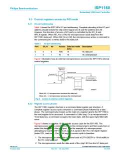
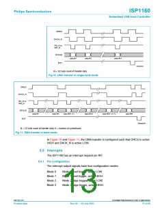
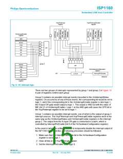
To further describe the complete access cycles of the internal control registers, the
status of some pins of the microprocessor bus interface are shown in Figure 8.
Signals
Valid status
Valid status
Valid status
0
1
0
0
0
0
CS_N
A0
RD_N = 1,
WR_N = 0
RD_N = 0 (read) or
WR_N = 0 (write)
RD_N = 0 (read) or
WR_N = 0 (write)
RD_N,
WR_N
Register data
(lower word)
Register data
(upper word)
data bus
Command code
004aaa370
Fig 8. Accessing HC control registers.
8.4 FIFO buffer RAM access by PIO mode
Since the ISP1160’s internal memory is structured as a FIFO buffer RAM, the FIFO
buffer RAM is mapped to dedicated register fields. Therefore, accessing the internal
FIFO buffer RAM is similar to accessing the internal control registers in multiple data
phases.
9397 750 11371
© Koninklijke Philips Electronics N.V. 2003. All rights reserved.
Product data
Rev. 04 — 04 July 2003
11 of 88

 NXP [ NXP ]