ISP1160
Embedded USB Host Controller
Philips Semiconductors
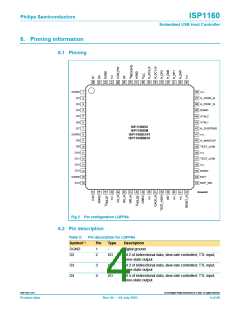
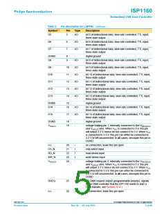
Table 2:
Pin description for LQFP64…continued
Symbol[1]
Pin
Type
Description
D5
5
I/O
bit 5 of bidirectional data; slew-rate controlled; TTL input;
three-state output
D6
D7
6
7
I/O
I/O
bit 6 of bidirectional data; slew-rate controlled; TTL input;
three-state output
bit 7 of bidirectional data; slew-rate controlled; TTL input;
three-state output
DGND
D8
8
9
-
digital ground
I/O
bit 8 of bidirectional data; slew-rate controlled; TTL input;
three-state output
D9
10
11
12
13
14
I/O
I/O
I/O
I/O
I/O
bit 9 of bidirectional data; slew-rate controlled; TTL input;
three-state output
D10
D11
D12
D13
bit 10 of bidirectional data; slew-rate controlled; TTL input;
three-state output
bit 11 of bidirectional data; slew-rate controlled; TTL input;
three-state output
bit 12 of bidirectional data; slew-rate controlled; TTL input;
three-state output
bit 13 of bidirectional data; slew-rate controlled; TTL input;
three-state output
DGND
D14
15
16
-
digital ground
I/O
bit 14 of bidirectional data; slew-rate controlled; TTL input;
three-state output
D15
17
I/O
bit 15 of bidirectional data; slew-rate controlled; TTL input;
three-state output
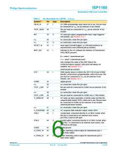
DGND
VHOLD1
18
19
-
-
digital ground
voltage holding pin 1; internally connected to the VREG(3V3)
and VHOLD2 pins. When VCC is connected to 5 V, this pin
will output 3.3 V, hence do not connect it to 5 V. When VCC
is connected to 3.3 V, this pin can either be connected to
3.3 V or left unconnected. In all cases, decouple this pin to
DGND.
n.c.
20
21
22
23
24
-
I
I
I
-
no connection; leave this pin open
chip select input
CS_N
RD_N
WR_N
VHOLD2
read strobe input
write strobe input
voltage holding pin 2; internally connected to the VREG(3V3)
and VHOLD1 pins. When VCC is connected to 5 V, this pin
will output 3.3 V, hence do not connect it to 5 V. When VCC
is connected to 3.3 V, this pin can either be connected to
3.3 V or left unconnected. In all cases, decouple this pin to
DGND.
DREQ
n.c.
25
26
O
-
HC DMA request output (programmable polarity); signals
to the DMA controller that the ISP1160 wants to start a
DMA transfer; see Section 10.4.1
no connection; leave this pin open
9397 750 11371
© Koninklijke Philips Electronics N.V. 2003. All rights reserved.
Product data
Rev. 04 — 04 July 2003
5 of 88

 NXP [ NXP ]