ISP1160
Embedded USB Host Controller
Philips Semiconductors
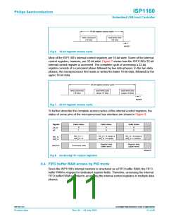
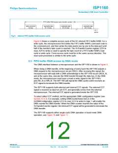
FIFO buffer RAM access cycle (transfer counter = 2N)
write command
(16 bits)
read/write data
#1 (16 bits)
read/write data
#2 (16 bits)
read/write data
#N (16 bits)
t
MGT941
Fig 9. Internal FIFO buffer RAM access cycle.
Figure 9 shows a complete access cycle of the HC internal FIFO buffer RAM. For a
write cycle, the microprocessor first writes the FIFO buffer RAM’s command code to
the command port, and then writes the data words one by one to the data port until
half of the transfer’s byte count is reached. The HcTransferCounter register (22H to
read, A2H to write) is used to specify the byte count of a FIFO buffer RAM’s read
cycle or write cycle. Every access cycle must be in the same access direction. The
read cycle procedure is similar to the write cycle.
8.5 FIFO buffer RAM access by DMA mode
The DMA interface between a microprocessor and the ISP1160 is shown in Figure 4.
When doing a DMA transfer, at the beginning of every burst the ISP1160 outputs a
DMA request to the microprocessor via pin DREQ. After receiving this signal, the
microprocessor will reply with a DMA acknowledge to the ISP1160 via pin DACK_N,
and at the same time, execute the DMA transfer through the data bus. In the DMA
mode, the microprocessor must issue a read or write signal to the ISP1160’s
pins RD_N or WR_N. The ISP1160 will repeat the DMA cycles until it receives an
EOT signal to terminate the DMA transfer.
The ISP1160 supports both external and internal EOT signals. The external EOT
signal is received as input on pin EOT, and generally comes from the external
microprocessor. The internal EOT signal is generated inside the ISP1160.
To select either EOT method, set the appropriate DMA configuration register (see
Section 10.4.2). For example, setting DMACounterSelect (bit 2) of the
HcDMAConfiguration register (21H to read, A1H to write) to logic 1 will enable the
DMA counter for DMA transfer. When the DMA counter reaches the value of the
HcTransferCounter register, the internal EOT signal will be generated to terminate the
DMA transfer.
The ISP1160 supports either single-cycle DMA operation or burst mode DMA
operation; see Figure 10 and Figure 11.
9397 750 11371
© Koninklijke Philips Electronics N.V. 2003. All rights reserved.
Product data
Rev. 04 — 04 July 2003
12 of 88

 NXP [ NXP ]