ISP1160
Embedded USB Host Controller
Philips Semiconductors
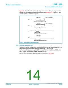
HcµPInterrupt
register
HcµPInterruptEnable
register
HcInterruptEnable
register
MIE
RHSC
FNO
UE
OR
RD
SF
SO
group 2
RHSC
FNO
UE
OR
HcHardwareConfiguration
register
RD
LE
INT
InterruptPinEnable
LATCH
SF
004aaa102
SO
HcInterruptStatus
register
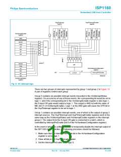
Fig 13. HC interrupt logic.
There are two groups of interrupts represented by group 1 and group 2 in Figure 13.
A pair of registers control each group.
Group 2 contains six possible interrupt events (recorded in the HcInterruptStatus
register). On occurrence of any of these events, the corresponding bit would be set to
logic 1; and if the corresponding bit in the HcInterruptEnable register is also logic 1,
the 6-input OR gate would output a logic 1. This output is AND-ed with the value of
MIE (bit 31 of HcInterruptEnable). Logic 1 at the AND gate will cause the OPR bit in
the HcµPInterrupt register to be set to logic 1.
Group 1 contains six possible interrupt events, one of which is the output of group 2
interrupt sources. The HcµPInterrupt and HcµPInterruptEnable registers work in the
same way as the HcInterruptStatus and HcInterruptEnable registers in the interrupt
group 2. The output from the 6-input OR gate is connected to a latch, which is
controlled by InterruptPinEnable (bit 0 of the HcHardwareConfiguration register).
In the event in which the software wishes to temporarily disable the interrupt output of
the ISP1160 Host Controller, the following procedure should be followed:
1. Make sure that the InterruptPinEnable bit in the HcHardwareConfiguration
register is set to logic 1.
2. Clear all bits in the HcµPInterrupt register.
3. Set the InterruptPinEnable bit to logic 0.
9397 750 11371
© Koninklijke Philips Electronics N.V. 2003. All rights reserved.
Product data
Rev. 04 — 04 July 2003
15 of 88

 NXP [ NXP ]