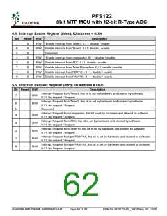
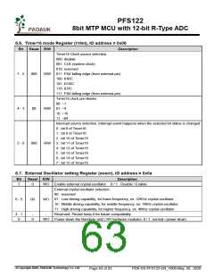
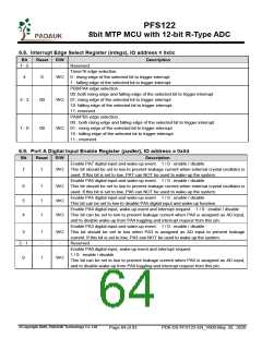
PFS122
8bit MTP MCU with 12-bit R-Type ADC
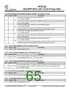
6.16. Port B Control Register (pbc), IO address = 0x16
Bit
Reset R/W
Description
Port B control register. This register is used to define input mode or output mode for each
corresponding pin of port B. 0 / 1: input / output
7 - 0
0x00 R/W
6.17. Port B Pull-High Register (pbph), IO address = 0x17
Bit
Reset R/W
Description
Port B pull-high register. This register is used to enable the internal pull-high device on each
7 - 0
0x00
R/W corresponding pin of port B and this pull high function is active only for input mode.
0 / 1 : disable / enable
6.18. Port B Pull-Low Register (pbpl), IO address = 0x18
Bit
Reset R/W
Description
7 -0
0x00 R/W PB pull-low register. 0 / 1: Disable / Enable.
6.19. ADC Control Register (adcc), IO address = 0x20
Bit
Reset
R/W
Description
Enable ADC function. 0/1: Disable/Enable.
7
0
R/W
ADC process control bit.
6
0
R/W
Write “1” to start conversion
Read “1” to indicate the ADC is ready or end of conversion.
Channel selector. These four bits are used to select input signal for AD conversion.
0000: PB0/AD0,
0001: PB1/AD1,
0010: PB2/AD2,
0011: PB3/AD3,
0100: PB4/AD4,
0101: PB5/AD5,
5 - 2
0000
R/W
0110: PB6/AD6,
0111: PB7/AD7,
1000: PA3/AD8,
1001: PA4/AD9,
1010: PA0/AD10,
1111: (Channel F) Bandgap reference voltage
Others: reserved
0 - 1
-
-
Reserved. (keep 0 for future compatibility)
©Copyright 2020, PADAUK Technology Co. Ltd
Page 66 of 93
PDK-DS-PFS122-EN_V000-May 28, 2020

 PADAUK [ PADAUK Technology ]