PFS122
8bit MTP MCU with 12-bit R-Type ADC
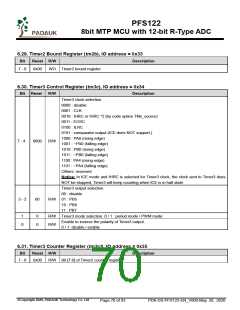
6.29. Timer2 Bound Register (tm2b), IO address = 0x33
Bit
Reset R/W
Description
7 - 0
0x00 WO Timer2 bound register.
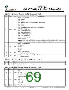
6.30. Timer3 Control Register (tm3c), IO address = 0x34
Bit Reset
R/W
Description
Timer3 clock selection.
0000 : disable
0001 : CLK
0010 : IHRC or IHRC *2 (by code option TMx_source)
0011 : EOSC
0100 : ILRC
0101 : comparator output (ICE does NOT support.)
1000 : PA0 (rising edge)
7 - 4
0000
R/W
1001 : ~PA0 (falling edge)
1010 : PB0 (rising edge)
1011 : ~PB0 (falling edge)
1100 : PA4 (rising edge)
1101 : ~PA4 (falling edge)
Others: reserved
Notice: In ICE mode and IHRC is selected for Timer3 clock, the clock sent to Timer3 does
NOT be stopped, Timer3 will keep counting when ICE is in halt state.
Timer3 output selection.
00 : disable
3 - 2
00
R/W 01 : PB5
10 : PB6
11 : PB7
1
0
0
0
R/W Timer3 mode selection. 0 / 1 : period mode / PWM mode
Enable to inverse the polarity of Timer3 output.
R/W
0 / 1: disable / enable
6.31. Timer3 Counter Register (tm3ct), IO address = 0x35
Bit
Reset R/W
0x00 R/W Bit [7:0] of Timer2 counter register.
Description
7 - 0
©Copyright 2020, PADAUK Technology Co. Ltd
Page 70 of 93
PDK-DS-PFS122-EN_V000-May 28, 2020

 PADAUK [ PADAUK Technology ]