PFS122
8bit MTP MCU with 12-bit R-Type ADC
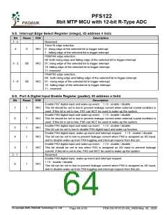
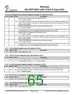
6.10.Port B Digital Input Enable Register (pbdier), IO address = 0x0e
Bit
Reset R/W
Description
Enable PB7~PB6 digital input and wake-up event.
1 / 0 : enable / disable
7 - 6
11
1
WO These bits can be set to low to prevent leakage current when PB7~PB6 are assigned as AD
inputs. When disable is selected, the wake-up function and interrupt requests from these
pins are also disabled.
Enable PB5 digital input, wake-up event and interrupt request.
1 / 0 : enable / disable
5
4 - 1
0
WO
This bit can be set to low to prevent leakage current when PB5 is assigned as AD input, and
to disable wake-up from PB5 toggling and interrupt request from this pin.
Enable PB47~PB1 digital input and wake-up event.
1 / 0 : enable / disable
1111
WO These bits can be set to low to prevent leakage current when PB4~PB1 are assigned as AD
inputs. When disable is selected, the wake-up function and interrupt requests from these
pins are also disabled.
Enable PB0 digital input, wake-up event and interrupt request.
1 / 0 : enable / disable
1
WO
This bit can be set to low to prevent leakage current when PB0 is assigned as AD input, and
to disable wake-up from PB0 toggling and interrupt request from this pin.
6.11. Port A Data Register (pa), IO address = 0x10
Bit
Reset R/W
0x00 R/W Data register for Port A.
Description
7 - 0
6.12. Port A Control Register (pac), IO address = 0x11
Bit
Reset R/W
Description
Port A control registers. This register is used to define input mode or output mode for each
corresponding pin of port A. 0 / 1: input / output
7 - 0
0x00 R/W
6.13. Port A Pull-High Register (paph), IO address = 0x12
Bit
Reset R/W
Description
Port A pull-high register. This register is used to enable the internal pull-high device on each
7 - 0
0x00 R/W corresponding pin of port A and this pull high function is active only for input mode.
0 / 1 : disable / enable
6.14. Port A Pull-Low Register (papl), IO address = 0x13
Bit
Reset R/W
Description
7 - 0
0x00 R/W PA pull-low register. 0 / 1: Disable / Enable.
6.15. Port B Data Register (pb), IO address = 0x15
Bit
Reset R/W
0x00 R/W Data register for Port B.
Description
7 - 0
©Copyright 2020, PADAUK Technology Co. Ltd
Page 65 of 93
PDK-DS-PFS122-EN_V000-May 28, 2020

 PADAUK [ PADAUK Technology ]