PFS122
8bit MTP MCU with 12-bit R-Type ADC
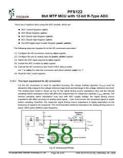
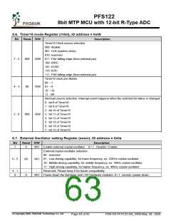
5.13.2 ADC clock selection
Before starting the AD conversion, the minimum signal acquisition time should be met for the selected
analog input signal, the selection of ADCLK must be met the minimum signal acquisition time.
The clock of ADC module (ADCLK) can be selected by adcm register; there are 8 possible options for
ADCLK from CLK÷1 to CLK÷128 (CLK is the system clock). Due to the signal acquisition time TACQ is one
clock period of ADCLK, the ADCLK must meet that requirement. The recommended ADC clock is to
operate at 2us.
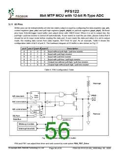
5.13.3 Configure the analog pins
There are 12 analog signals can be selected for AD conversion, 11 analog input signals come from
external pins and one is from internal bandgap reference voltage 1.2V. For those external pins defined as
analog input, to avoid leakage current from the digital circuit of the shared IO ports, please always
remember to disable the digital input function (set the corresponding bit of padier or pbdier register to be
0).
Due to the measurement signals of ADC are very small; user should avoid the measured signal to be
interfered during the measurement period. Thus, the selected pin should: (1)be set to input mode; (2) turn
off weak pull-high and pull-low resistor; (3) set the corresponding pin to analog input by port A/B digital
input disable register (padier / pbdier).
5.13.4 Using the ADC
The following example shows how to use ADC with PB0~PB3:
First, defining the selected pins:
PBC
=
=
=
=
0B_XXXX_0000;
0B_XXXX_0000;
0B_XXXX_0000;
0B_XXXX_0000;
//
//
//
//
PB0 ~ PB3 as Input
PBPH
PBPL
PBDIER
PB0 ~ PB3 without pull-high resistor
PB0 ~ PB3 without pull-low resistor
PB0 ~ PB3 digital input is disabled
Next, setting ADCC register, example as below:
$
$
$
ADCC Enable, PB3;
ADCC Enable, PB2;
ADCC Enable, PB0;
//
//
//
set PB3 as ADC input
set PB2 as ADC input
set PB0 as ADC input
Next, setting ADCM register, example as below:
$
$
ADCM /16;
ADCM /8;
//
//
recommend /16 @System Clock=8MHz
recommend /8 @System Clock=4MHz
Then, start the ADC conversion:
AD_START = 1;
// start ADC conversion
while(!AD_DONE) NULL;
// wait ADC conversion result
Finally, it can read ADC result when AD_DONE is high:
WORD
Data$1
Data;
ADCRH;
//
two bytes result: ADCRH and ADCRL
=
©Copyright 2020, PADAUK Technology Co. Ltd
Page 59 of 93
PDK-DS-PFS122-EN_V000-May 28, 2020

 PADAUK [ PADAUK Technology ]