PFS122
8bit MTP MCU with 12-bit R-Type ADC
Data$0
Data
=
=
ADCRL;
Data >> 4;
The ADC can be disabled by using the following method:
ADCC Disable;
$
or
ADCC
=
0;
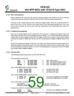
5.13.5 How to calculate ADC input voltage VIN
For PFS122, only VDD but not 1.2V bandgap voltage can be selected as the VREF of the ADC. When VDD
is not regulated, users have to use the reading of 1.2V bandgap voltage to deduce the input voltage (VIN)
by the ratio of the readings. The principle is as below:
VBG / VDD = NBG / 4096 ....(1)
VIN / VDD = NIN / 4096 ....(2)
Where VIN is the analog input voltage
VBG is the 1.2V bandgap voltage
NIN is the corresponding ADC reading of VIN
N
BG is the corresponding ADC reading of VBG
VDD is the VDD at the measuring instant
4096 is the full swing reading when VIN=VDD (12bit: 212 = 4096)
(2)/(1) we get
VIN/VBG = NIN/NBG
And so
VIN = NIN / NBG *VBG
It means users can firstly get the readings for VIN and VBG respectively in a very short period that VDD
remains unchanged. And then use multiplication and division program module or use look-up table
method to finally get the VIN voltage.
If necessary, please contact FAE for demo code reference.
©Copyright 2020, PADAUK Technology Co. Ltd
Page 60 of 93
PDK-DS-PFS122-EN_V000-May 28, 2020

 PADAUK [ PADAUK Technology ]