PFS122
8bit MTP MCU with 12-bit R-Type ADC
5.11 IO Pins
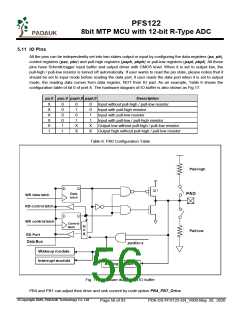
All the pins can be independently set into two states output or input by configuring the data registers (pa, pb),
control registers (pac, pbc) and pull-high registers (paph, pbph) or pull-low registers (papl, pbpl). All these
pins have Schmitt-trigger input buffer and output driver with CMOS level. When it is set to output low, the
pull-high / pull-low resistor is turned off automatically. If user wants to read the pin state, please notice that it
should be set to input mode before reading the data port; if user reads the data port when it is set to output
mode, the reading data comes from data register, NOT from IO pad. As an example, Table 6 shows the
configuration table of bit 0 of port A. The hardware diagram of IO buffer is also shown as Fig.17.
pa.0 pac.0 paph.0 papl.0
Description
X
X
X
X
0
0
0
0
0
1
1
0
1
0
1
X
X
0
0
1
1
X
X
Input without pull-high / pull-low resistor
Input with pull-high resistor
Input with pull-low resistor
Input with pull-low / pull-high rseistor
Output low without pull-high / pull-low resistor
Output high without pull-high / pull-low resistor
1
Table 6: PA0 Configuration Table
Fig. 17: Hardware diagram of IO buffer
PB4 and PB7 can adjust their drive and sink current by code option PB4_PB7_Drive.
©Copyright 2020, PADAUK Technology Co. Ltd
Page 56 of 93
PDK-DS-PFS122-EN_V000-May 28, 2020

 PADAUK [ PADAUK Technology ]