OXCB950
OXFORD SEMICONDUCTOR LTD.
9 COMPLIANCE TO PC CARD STANDARDS, 7.0 AND 7.1
This section is relevant only to the cardbus application
of the OXCB950.
pulldown resistor. This is compatible with PC Card
Standards 7.0, and all PC Card Standards prior to the
release of version 7.1.
The OXCB950 requires the presence of the PCI_CLK for
reliable operation of the internal UART. Since the presence
of the pci clk is governed by the cardbus connector signal
CCLKRUN# then, for full functionality, this connector pin
must be kept asserted to ensure that the pci_clk is not
stopped. The OXCB950 is, however, tolerant to fluctuations
in the pci clk line.
PC Card Standard 7.1, however, does not allow the use of
this pulldown for new designs and all new designs that are
not tolerant to the clock stopping are required to implement
the clock run protocol on the CCLKRUN# line.
The clock run protocol can be implemented externally
through the use of the following circuitry and allows the
OXCB950 part to be compliant to version 7.1 of the PC
Card Standard.
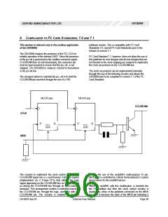
The cheapest option to maintain the pci_clk is to hold the
CCLKRUN# pin asserted through the use of a 1K0
74LV74 (so)
74LV74 (so)
CCLKRUN#
CCLK
MIO0
D
Q
D
Q
CLR
CLR
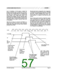
The circuitry to implement the clock control logic on the
CCLKRUN# signal line is a synchronous 2-bit shift register
(implemented via 2 D-type FF's) that utilises the logic
signal appearing on the CCLKRUN# line as DATA, as well
as driving the CCLKRUN# line through an open-collector
transistor. This arrangement creates a controlled loop from
the CCLKRUN# pin, through the logic, and back onto the
CCLKRUN# pin. The circuitry is enabled or disabled
through the use of the oxcb950's multi-purpose IO pin,
MIO0, that is controlled by Oxford Semiconductor's custom
device-driver for the oxcb950 device.
When the oxcb950, with this modification, is inserted into
the PC cardbus slot then the clock control circuitry is
disabled by virtue of the pulldown connected on the MIO0
pin. This is because the state of the MIO0 pin following a
DS-0033 Sep 05
External-Free Release
Page 56

 OXFORD [ OXFORD SEMICONDUCTOR ]