OXCB950
OXFORD SEMICONDUCTOR LTD.
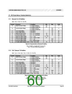
11 DC ELECTRICAL CHARACTERISTICS
11.1 Normal 3.3v I/O Buffers
Vdd = 3.3v +/- 0.3v, Ta = 0 to 70c
Symbol Parameter
Condition
Min
2.0
2.0
Max
Units
1
VIH
High level input voltage
LVCMOS Interface
V
1
1
LVCMOS Schmitt trig
1
VIL
Low level input voltage
LVCMOS Interface
0.8
0.8
4.0
4.0
10
V
LVCMOS Schmitt trig
See Note 2
CIN
COUT
IIH
Cap of input buffers
pF
pF
µA
µA
V
Cap of output buffers
High level input current
Low level input current
High level output voltage
High level output voltage
Low level output voltage
Low level output voltage
See Note 2
Vin = VDD, no pull-ups.
Vin = VSS, no pull-ups
-10
IIL
-10
10
VDD – 0.05
VOH
VOH
VOL
VOL
IOZ
IOH = -1 µA
IOH = -1mA to -12mA
OL = 1 µA
IOL = 1mA to 12 mA
2.4
V
0.05
0.4
10
V
I
V
Tri-state output leakage current Vout = Vss or Vdd
-10
µA
Table 29: Characteristics of Normal I/O buffers
Note 1: LVCMOS is compatible with TTL levels at 3.3v
Note 2: This value excludes package parasitics
11.2 5.0v Tolerant I/O Buffers
Vdd = 3.3v +/- 0.3v, Vext = 5.0v +/- 0.25v, Ta = 0 to 70c
Symbol Parameter
Condition
Min
2.0
2.0
Max
Units
2
1
VIH
High level input voltage
LVCMOS Interface
V
1
1
LVCMOS Schmitt trig
2
1
VIL
Low level input voltage
LVCMOS Interface
0.8
0.8
4.0
4.0
10
V
LVCMOS Schmitt trig
See Note 3
CIN
COUT
IIH
Cap of input buffers
pF
pF
µA
µA
V
Cap of output buffers
High level input current
Low level input current
High level output voltage
High level output voltage
Low level output voltage
Low level output voltage
See Note 3
Vin = VDD, no pull-ups.
Vin = VSS, no pull-ups
-10
IIL
-10
10
VDD – 0.05
VOH
VOH
VOL
VOL
IOZ
I
OH = -1 µA
IOH = -1mA to -6mA
IOL = 1 µA
2.4
V
0.05
0.4
10
V
IOL = 1mA to 6 mA
V
Tri-state output leakage current Vout = Vss or Vext
-10
µA
Table 32: Characteristics of 5v tolerant I/O buffers
Note 1: LVCMOS is compatible with TTL levels at 3.3v
Note 2: All 5v tolerant inputs have less than 0.2v hysteresis
Note 3: This value excludes package parasitics
OXCB950 DataSheet
MIS-0004 Jul 04 External-Free Release
Page 60

 OXFORD [ OXFORD SEMICONDUCTOR ]