OXCB950
OXFORD SEMICONDUCTOR LTD.
Function Access Examples
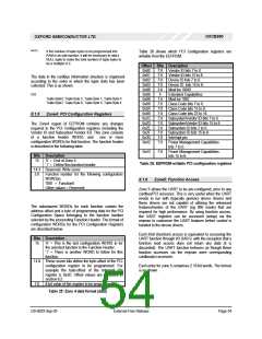
Word Bits Description
15
‘1’ - another WORD to follow
1) Enable Internal loopback (Enable bit 4, MCR register)
14:1 BAR number to access
2
000 for BAR 0 (UART IO BAR)
1000100000000100
1000000000010000
Others values are reserved
‘0’ : Read access required
(data will be discarded)
11
st
1 Word: BAR No = 000 (UART), Write Access,
‘1’ : Write access required
Address=00000100 (MCR reg).
10:8 Reserved – write 0’s
nd
2
Word: Data to be written=00010000
7:0
I/O address to access
This is the address that needs to be
written/read and is the offset address from the
specified BAR.
2) Enable FIFO (Enable bit 0, FCR register)
1000100000000010
1000000000000001
E.g to access SPR register of UART, address
is 00000111 (7dec).
st
1 Word: BAR No = 000 (UART), Write access,
st
1 WORD of FUNCTION ACCESS PAIR
address=00000010 (FCR reg)
nd
2
Word: Data to be written=00000001
Word Bits Description
3) Read IER Register
15
‘1’ – another function access WORD pair to
follow.
1000000000000001
‘0’ – no more function access word pairs.
(End EEPROM program)
1000000000000000
14:8 Reserved – write 0’s
st
1 Word: BAR No =000 (UART), Read access,
7:0
Data to be written to specified address.
address=00000001 (IER reg)
nd
Field is unused for function access READS
2
Word: No data to be written (as read access). Read
(set to 0’s for reads)
data is discarded
nd
2
WORD of FUNCTION ACCESS PAIR
DS-0033 Sep 05
External-Free Release
Page 55

 OXFORD [ OXFORD SEMICONDUCTOR ]