OXCB950
OXFORD SEMICONDUCTOR LTD.
NOTE1
If the number of tuple bytes to be programmed into
RAM is an odd number, it will be necessary to add a
NULL tuple to make the total number of tuple bytes to
be a multiple of 2.
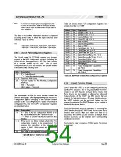
Table 26 shows which PCI Configuration registers are
writable from the EEPROM.
Offset Bits Description
0x00
0x01
0x02
0x03
0x06
0x06
0x06
0x09
0x0A
0x0B
0x2C
0x2D
0x2E
0x2F
0x3D
0x42
7:0 Vendor ID bits 7 to 0.
7:0 Vendor ID bits 15 to 8.
7:0 Device ID bits 7 to 0.
7:0 Device ID bits 15 to 8.
3:0 Must be ‘0000’.
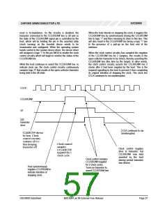
The data in the cardbus information structure is organised
according to the order in which the tuple data has been
collected. This is as shown
CIS :
4
Extended Capabilities.
Tuple Byte3, Tuple Byte 2, Tuple Byte 1, Tuple Byte 0
Tuple Byte7, Tuple Byte 6, Tuple Byte 5, Tuple Byte 4
7:5 Must be ‘000’.
7:0 Class Code bits 7 to 0.
7:0 Class Code bits 15 to 8.
7:0 Class Code bits 23 to 16.
7:0 SubsystemVendor ID bits 7 to 0.
7:0 SubsystemVendor ID bits 15 to 8.
7:0 Subsystem ID bits 7 to 0.
7:0 Subsystem ID bits 15 to 8.
7:0 Interrupt pin.
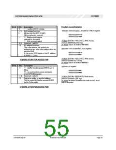
8.1.5 Zone4: PCI Configuration Registers
The Zone4 region of EEPROM contains any changes
required to the PCI Configuration registers (including the
Vendor ID and Subsystem Vendor ID). This zone consists
of a function header WORD, and
one or more
configuration WORDs for that function. The function header
is described in the following table.
7:0 Power Management Capabilities
bits 7 to 0.
0x43
7:0 Power Management Capabilities
bits 15 to 8.
Bits Description
15
‘0’ = End of Zone 4.
Table 26: EEPROM-writable PCI configuration registers
‘1’ = Define this function header.
14:3 Reserved. Write zeros.
2:0 Function number for the following configuration
WORD(s).
8.1.6 Zone5: Function Access
‘000’ = Function0
Other values = Reserved.
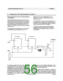
Zone 5 allows the UART to be pre-configured, prior to any
cardbus/PCI accesses. This is very useful when the UART
needs to run with (typically generic) device drivers and
these drivers are not capable of utilising the enhanced
features/modes of the UART (eg 950 mode) that are
required for high performance. By using function access,
the UART registers can be accessed (setup) via the
eeprom to customize the UART features before control is
handed to the device drivers.
The subsequent WORDs for each function contain the
address offset and a byte of programming data for the PCI
Configuration Space belonging to the function number
selected by the proceeding Function-Header. The format of
configuration WORDs for the PCI Configuration Registers
are described below.
Each 8-bit (function) access is equivalent to accessing the
UART function through I/O BAR 0, with the exception that a
function read access does not return any data (it is
discarded). The UART function behaves as though these
function accesses via the eeprom were corresponding
cardbus/pci accesses.
Bits Description
15
‘0’ = This is the last configuration WORD in for
the selected function in the Function-Header.
‘1’ = There is another WORD to follow for this
function.
14:8 These seven bits define the byte-offset of the PCI
configuration register to be programmed. For
example the byte-offset of the Interrupt Pin
register is 0x3D. Offset values are tabulated in
section 6.2.
Each entry for zone 5 comprises 2 16 bit words. The format
is as shown.
7:0 8-bit value of the register to be programmed
Table 25: Zone 4 data format (data)
DS-0033 Sep 05
External-Free Release
Page 54

 OXFORD [ OXFORD SEMICONDUCTOR ]