OXCB950
OXFORD SEMICONDUCTOR LTD.
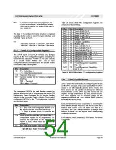
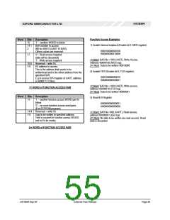
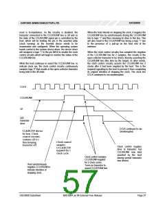
Now that the target has signalled that the clock is to be
maintained, the target's drive on the CCLKRUN# line must
be maintained for 2 clock cycles during which time the host
will begin to drive the line also. Since the CCLKRUN# is
also the data to the 2-bit shift register then, when the
CCLKRUN# is driven by the control circuitry, it will take 2
clock cycles for the new clock run status to propagate
through the logic to turn off the transistor. During this
period, the host will have detected the assertion of the
CCLKRUN# by the target and will also begin to assert the
CLKRUN# line, so that when the clock control's transistor is
turned off, the CCLKRUN# will be held in the asserted
state by the host thereby keeping the transistor off. The
transistor will remain off until the host next attempts to
negate the CCLKRUN# line to indicate a clock stop and is
prevented from doing so by the clock control logic.
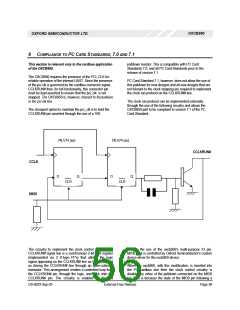
For the condition when the device driver needs to place the
OXCB950 into
a low powerstate (such as Power
Management States D2, D3) for which the clock control
logic is not required, then the device driver will assign the
MIO0 pin to a logic 0 that disables the clock control circuitry
and forces the clockrun transistor to the off state. For this
condition, when the host negates the CCLKRUN# line it
does not see the CCLKRUN# being asserted by the target
(as the circuitry has been disabled) and the clock is
stopped by the host after the relevant number of clocks
from the negation.
For these low powerstate conditions, any Power
Management Events will assert the PME# (CSYSCHG) line
that will result in the host asserting the CCLKRUN# line
and restarting the clock. The power management enabled
device driver will then enable the clock control circuitry to
maintain the clock to service this event.
OXCB950 DataSheet
MIS-0004 Jul 04 External-Free Release
Page 58

 OXFORD [ OXFORD SEMICONDUCTOR ]