OXCB950
OXFORD SEMICONDUCTOR LTD.
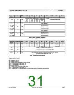
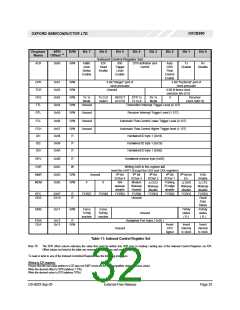
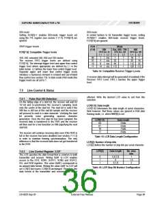
Register
Name
SPR
R/W
Bit 7
Bit 6
Bit 5
Bit 4
Bit 3
Bit 2
Bit 1
Bit 0
Offset 10
Indexed Control Register Set
ACR
0x00
R/W
Addit-
ional
ICR
Read
950
DTR definition and
control
Auto
DSR
Tx
Rx
Trigger
Level
Disable
Disable
Status
Enable
Enable
Flow
Enable
Control
Enable
CPR
TCR
CKS
TTL
0x01
0x02
0x03
0x04
0x05
R/W
R/W
R/W
R/W
R/W
5 Bit “integer” part of
clock prescaler
Unused
3 Bit “fractional” part of
clock prescaler
4 Bit N-times clock
selection bits [3:0]
Tx 1x
Mode
Tx CLK
BDOUT
on DTR
DTR 1x
Tx CLK
Rx 1x
Mode
0
Receiver
Select
Clock Sel[1:0]
Unused
Transmitter Interrupt Trigger Level (0-127)
RTL
Unused
Unused
Unused
Receiver Interrupt Trigger Level (1-127)
FCL
0x06
R/W
Automatic Flow Control Lower Trigger Level (0-127)
FCH
ID1
ID2
ID3
0x07
0x08
0x09
0x0A
R/W
R
Automatic Flow Control Higher Trigger level (1-127)
Hardwired ID byte 1 (0x16)
R
Hardwired ID byte 1 (0xC9)
R
Hardwired ID byte 1 (0x50)
REV
0x0B
R
Hardwired revision byte (0x05)
CSR
NMR
MDM
0x0C
0x0D
0x0E
W
Writing 0x00 to this register will
reset the UART (Except the CKS and CKA registers)
R/W
R/W
Unused
9th Bit
SChar 4
SIN
9th Bit
9th Bit
9th Bit
SChar 1
Trailing
RI edge
disable
9th-bit Int.
9 Bit
SChar 3
Modem
Wakeup
Disable
SChar 2
En.
Enable
0
0
∆ DCD
Wakeup
disable
FCR[3]
∆ DSR
Wakeup
disable
FCR[1]
∆ CTS
Wakeup
disable
FCR[0]
Good
wakeup
disable
RFC
GDS
0X0F
0X10
R
R
FCR[7]
FCR[6]
FCR[5]
FCR[4]
Unused
FCR[2]
Data
Status
RxRdy
status
( R )
DMS
0x11
R/W
Force
TxRdy
inactive
Force
RxRdy
inactive
TxRdy
status
( R )
Unused
Hardwired Port Index ( 0x00 )
PIDX
CKA
0x12
0x13
R
R/W
Invert
DTR
Invert
internal
tx clock
Invert
internal
rx clock
Unused
signal
Table 11: Indexed Control Register Set
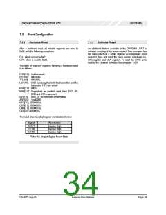
Note 10: The SPR offset column indicates the value that must be written into SPR prior to reading / writing any of the Indexed Control Registers via ICR.
Offset values not listed in the table are reserved for future use and must not be used.
To read or write to any of the Indexed Controlled Registers use the following procedure:
Writing to ICR registers:
Ensure that the last value written to LCR was not 0xBF (reserved for 650 compatible register access value).
Write the desired offset to SPR (address 111b).
Write the desired value to ICR (address 101b).
DS-0033 Sep 05
External-Free Release
Page 32

 OXFORD [ OXFORD SEMICONDUCTOR ]