NCV5171
Output Capacitor Selection
V
ripple
CC
I
I
IN
V
ripple
OUT
L
I
L
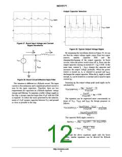
Figure 27. Boost Input Voltage and Current
Ripple Waveforms
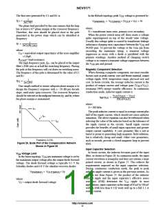
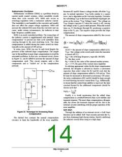
Figure 29. Typical Output Voltage Ripple
I
I
L
IN
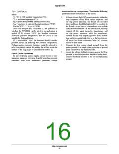
By examining the waveforms shown in Figure 29, we can
see that the output voltage ripple comes from two major
sources,
namely
capacitor
ESR
and
the
+
−
charging/discharging of the output capacitor. In boost
V
C
IN
CC
circuits, when the power switch turns off, I flows into the
L
output capacitor causing an instant DV = I × ESR. At the
IN
R
ESR
same time, current I − I
charges the capacitor and
L
OUT
increases the output voltage gradually. When the power
switch is turned on, I is shunted to ground and I
L
OUT
discharges the output capacitor. When the I ripple is small
L
enough, I can be treated as a constant and is equal to input
L
current I .
IN
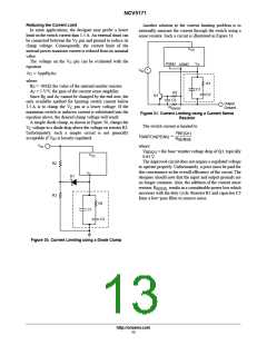
Figure 28. Boost Circuit Effective Input Filter
Summing up, the output voltage peak−peak ripple can be
calculated by:
The situation is different in a flyback circuit. The input
current is discontinuous and a significant pulsed current is
seen by the input capacitors. Therefore, there are two
requirements for capacitors in a flyback regulator: energy
storage and filtering. To maintain a stable voltage supply to
the chip, a storage capacitor larger than 20 mF with low ESR
is required. To reduce the noise generated by the inductor,
(I * I
(1 * D)
(f)
IN
OUT)
OUT)
V
+
OUT(RIPPLE)
(C
I
D
OUT
(C
)
) I ESR
IN
)(f)
OUT
The equation can be expressed more conveniently in
insert a 1.0 mF ceramic capacitor between V and ground
CC
terms of V , V
and I
for design purposes as
CC
OUT
OUT
as close as possible to the chip.
follows:
I
(V
OUT OUT
* V
)(f)
)
CC
1
OUT
V
+
OUT(RIPPLE)
(C
(C
)(f)
OUT
(I
)(V
V
)(ESR)
OUT OUT
)
CC
The capacitor RMS ripple current is:
Ǹ
2
2
) (D)
OUT
I
+
(I * I
) (1 * D))(I
OUT
RIPPLE
IN
V
OUT
V
* V
CC
OUT Ǹ
+ I
CC
Although the above equations apply only for boost
circuits, similar equations can be derived for flyback
circuits.
http://onsemi.com
12

 ONSEMI [ ONSEMI ]