NCV5171
APPLICATIONS INFORMATION
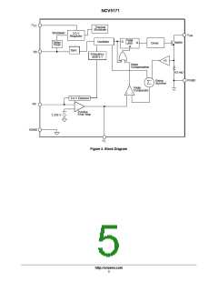
THEORY OF OPERATION
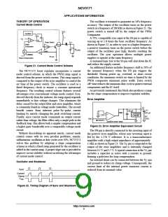
Current Mode Control
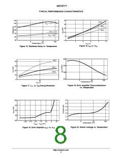
The oscillator is trimmed to guarantee an 18% frequency
accuracy. The output of the oscillator turns on the power
switch at a frequency of 280 kHz as shown in Figure 21. The
power switch is turned off by the output of the PWM
Comparator.
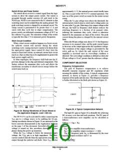
A TTL−compatible sync input at the SS pin is capable of
syncing up to 1.8 times the base oscillator frequency. As
shown in Figure 22, in order to sync to a higher frequency,
a positive transition turns on the power switch before the
output of the oscillator goes high, thereby resetting the
oscillator. The sync operation allows multiple power
supplies to operate at the same frequency.
V
CC
L
Oscillator
S
Q
−
V
C
R
+
Power Switch
D1
PWM
V
SW
Comparator
In Out
Driver
C
O
R
LOAD
X5
SUMMER
63 mW
Slope Compensation
A sustained logic low at the SS pin will shut down the IC
and reduce the supply current.
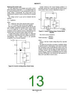
Figure 21. Current Mode Control Scheme
An additional feature includes frequency shift to 20% of
the nominal frequency when the FB pin triggers the
threshold. During power up, overload, or short circuit
conditions, the minimum switch on−time is limited by the
PWM comparator minimum pulse width. Extra switch
off−time reduces the minimum duty cycle to protect external
components and the IC itself.
The NCV5171 boost regulator incorporates a current
mode control scheme, in which the PWM ramp signal is
derived from the power switch current. This ramp signal is
compared to the output of the error amplifier to control the
on−time of the power switch. The oscillator is used as a
fixed−frequency clock to ensure a constant operational
frequency. The resulting control scheme features several
advantages over conventional voltage mode control. First,
derived directly from the inductor, the ramp signal responds
immediately to line voltage changes. This eliminates the
delay caused by the output filter and error amplifier, which
is commonly found in voltage mode controllers. The second
benefit comes from inherent pulse−by−pulse current
limiting by merely clamping the peak switching current.
Finally, since current mode commands an output current
rather than voltage, the filter offers only a single pole to the
feedback loop. This allows both a simpler compensation and
a higher gain−bandwidth over a comparable voltage mode
circuit.
Without discrediting its apparent merits, current mode
control comes with its own peculiar problems, mainly,
subharmonic oscillation at duty cycles over 50%. NCV5171
solves this problem by adopting a slope compensation
scheme in which a fixed ramp generated by the oscillator is
added to the current ramp. A proper slope rate is provided to
improve circuit stability without sacrificing the advantages
of current mode control.
As previously mentioned, this block also produces a ramp
for the slope compensation to improve regulator stability.
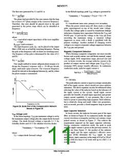
Error Amplifier
V
C
C1
120 pF
1MW
0.01 mF
Voltage
Clamp
+
−
1.276 V
NCV5171
R1
5 kW
FB
positive error−amp
Figure 23. Error Amplifier Equivalent Circuit
The FB pin is directly connected to the inverting input of
the positive error amplifier, whose non−inverting input is
fed by the 1.276 V reference. It is a transconductance
amplifier with a high output impedance of approximately
1 MW, as shown in Figure 23. The V pin is connected to the
C
output of the error amplifiers and is internally clamped
between 0.5 V and 1.7 V. A typical connection at the V pin
C
includes a capacitor in series with a resistor to ground,
forming a pole/zero for loop compensation.
An external shunt can be connected between the V pin
C
Oscillator and Shutdown
and ground to reduce its clamp voltage. Consequently, the
current limit of the internal power transistor current is
reduced from its nominal value.
Sync
Current
Ramp
V
SW
Figure 22. Timing Diagram of Sync and Shutdown
http://onsemi.com
9

 ONSEMI [ ONSEMI ]