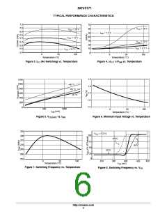
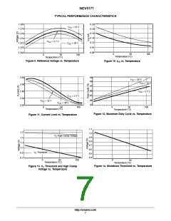
NCV5171
Switch Driver and Power Switch
approximately 1.5 V, the internal power switch briefly turns
on. This is a part of the NCV5171’s normal operation. The
turn−on of the power switch accounts for the initial current
swing.
The switch driver receives a control signal from the logic
section to drive the output power switch. The switch is
grounded through emitter resistors (63 mW total) to the
PGND pin. PGND is not connected to the IC substrate so that
switching noise can be isolated from the analog ground. The
peak switching current is clamped by an internal circuit. The
clamp current is guaranteed to be greater than 1.5 A and
varies with duty cycle due to slope compensation. The
power switch can withstand a maximum voltage of 40 V on
When the V pin voltage rises above the threshold, the
C
internal power switch starts to switch and a voltage pulse can
be seen at the V pin. Detecting a low output voltage at the
SW
FB pin, the built−in frequency shift feature reduces the
switching frequency to a fraction of its nominal value,
reducing the minimum duty cycle, which is otherwise
limited by the minimum on−time of the switch. The peak
current during this phase is clamped by the internal current
limit.
When the FB pin voltage rises above 0.4 V, the frequency
increases to its nominal value, and the peak current begins
to decrease as the output approaches the regulation voltage.
The overshoot of the output voltage is prevented by the
active pull−on, by which the sink current of the error
amplifier is increased once an overvoltage condition is
detected. The overvoltage condition is defined as when the
FB pin voltage is 50 mV greater than the reference voltage.
the collector (V pin). The saturation voltage of the switch
SW
is typically less than 1 V to minimize power dissipation.
Short Circuit Condition
When a short circuit condition happens in a boost circuit,
the inductor current will increase during the whole
switching cycle, causing excessive current to be drawn from
the input power supply. Since control ICs don’t have the
means to limit load current, an external current limit circuit
(such as a fuse or relay) has to be implemented to protect the
load, power supply and ICs.
In other topologies, the frequency shift built into the IC
prevents damage to the chip and external components. This
feature reduces the minimum duty cycle and allows the
transformer secondary to absorb excess energy before the
switch turns back on.
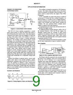
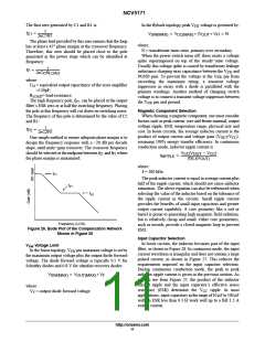
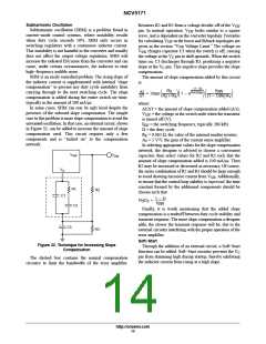
COMPONENT SELECTION
Frequency Compensation
The goal of frequency compensation is to achieve
desirable transient response and DC regulation while
ensuring the stability of the system. A typical compensation
network, as shown in Figure 25, provides a frequency
response of two poles and one zero. This frequency response
is further illustrated in the Bode plot shown in Figure 26.
I
L
V
OUT
V
C
R1
V
CC
CS5171
C2
V
C
C1
GND
Figure 25. A Typical Compensation Network
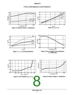
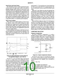
Figure 24. Startup Waveforms of Circuit Shown in
the Application Diagram. Load = 400 mA.
The high DC gain in Figure 26 is desirable for achieving
DC accuracy over line and load variations. The DC gain of
a transconductance error amplifier can be calculated as
follows:
The NCV5171 can be activated by either connecting the
V
pin to a voltage source or by enabling the SS pin.
CC
Startup waveforms shown in Figure 24 are measured in the
boost converter demonstrated in the Application Diagram
on the page 2 of this document. Recorded after the input
voltage is turned on, this waveform shows the various
phases during the power up transition.
Gain
DC
+ G R
M O
where:
= error amplifier transconductance;
G
M
R = error amplifier output resistance ≈ 1 MW.
O
When the V voltage is below the minimum supply
The low frequency pole, f is determined by the error
CC
P1,
voltage, the V
pin is in high impedance. Therefore,
amplifier output resistance and C1 as:
SW
current conducts directly from the input power source to the
output through the inductor and diode. Once V reaches
1
f
+
P1
CC
2pC1R
O
http://onsemi.com
10

 ONSEMI [ ONSEMI ]