NCV5171
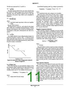
This circuit, shown in Figure 33, requires a minimum
when the switch is turned off. The specifications section of
number of components and allows the Soft−Start circuitry to
activate any time the SS pin is used to restart the converter.
this datasheet reveals that the typical operating current, I ,
Q
due to this circuitry is 5.5 mA. Additional guidance can be
found in the graph of operating current vs. temperature. This
graph shows that IQ is strongly dependent on input voltage,
V
IN
V , and temperature. Then
IN
V
V
CC
C
P
BIAS
+ V
I
IN Q
SS
Since the onboard switch is an NPN transistor, the base
drive current must be factored in as well. This current is
SS
drawn from the V pin, in addition to the control circuitry
IN
current. The base drive current is listed in the specifications
as DI /DI , or switch transconductance. As before, the
CC
SW
designer will find additional guidance in the graphs. With
that information, the designer can calculate
D2
D1
R1
I
DI
CC
SW
C1
P
+ V
I
D
DRIVER
IN SW
C2
C3
where:
= the current through the switch;
I
SW
D = the duty cycle or percentage of switch on−time.
and D are dependent on the type of converter. In a
I
SW
boost converter,
Figure 33. Soft Start
1
I
^ I
D
SW(AVG)
LOAD
Efficiency
Resistor R1 and capacitors C1 and C2 form the
compensation network. At turn on, the voltage at the V pin
starts to come up, charging capacitor C3 through Schottky
C
V
* V
IN
OUT
OUT
V
D ^
diode D2, clamping the voltage at the V pin such that
C
In a flyback converter,
switching begins when V reaches the V threshold,
C
C
V
I
OUT LOAD
1
typically 1.05 V (refer to graphs for detail over temperature).
I
^
SW(AVG)
V
IN
Efficiency
V
C
+ V
F(D2)
)V
C3
V
OUT
Therefore, C3 slows the startup of the circuit by limiting
D ^
N
V
)
S V
IN
N
P
OUT
the voltage on the V pin. The Soft−Start time increases with
C
the size of C3.
The switch saturation voltage, V , is the last major
(CE)SAT
Diode D1 discharges C3 when SS is low. If the shutdown
function is not used with this part, the cathode of D1 should
source of on−chip power loss.
collector−emitter voltage of the internal NPN transistor
when it is driven into saturation by its base drive current. The
V
is the
(CE)SAT
be connected to V .
IN
value for V
can be obtained from the specifications
(CE)SAT
Calculating Junction Temperature
or from the graphs, as “Switch Saturation Voltage.” Thus,
To ensure safe operation of NCV5171, the designer must
calculate the on−chip power dissipation and determine its
expected junction temperature. Internal thermal protection
circuitry will turn the part off once the junction temperature
exceeds 180°C 30°. However, repeated operation at such
high temperatures will ensure a reduced operating life.
Calculation of the junction temperature is an imprecise
but simple task. First, the power losses must be quantified.
There are three major sources of power loss on the
NCV5171:
P
^ V D
I
SAT
(CE)SAT SW
Finally, the total on−chip power losses are
P
D
+ P
BIAS
)P )P
DRIVER SAT
Power dissipation in a semiconductor device results in the
generation of heat in the junctions at the surface of the chip.
This heat is transferred to the surface of the IC package, but
a thermal gradient exists due to the resistive properties of the
package molding compound. The magnitude of the thermal
gradient is expressed in manufacturers’ data sheets as q
or junction−to−ambient thermal resistance. The on−chip
junction temperature can be calculated if q , the air
temperature near the surface of the IC, and the on−chip
power dissipation are known.
,
JA
• biasing of internal control circuitry, P
BIAS
• switch driver, P
DRIVER
JA
• switch saturation, P
SAT
The internal control circuitry, including the oscillator and
linear regulator, requires a small amount of power even
http://onsemi.com
15

 ONSEMI [ ONSEMI ]