NCV5171
The first zero generated by C1 and R1 is:
In the flyback topology, peak V voltage is governed by:
SW
1
f
+
V
+ V
CC(MAX)
)(V
)V ) N
Z1
SW(MAX)
OUT
F
2pC1R1
The phase lead provided by this zero ensures that the loop
where:
has at least a 45° phase margin at the crossover frequency.
Therefore, this zero should be placed close to the pole
generated in the power stage which can be identified at
frequency:
N = transformer turns ratio, primary over secondary.
When the power switch turns off, there exists a voltage
spike superimposed on top of the steady−state voltage.
Usually this voltage spike is caused by transformer leakage
inductance charging stray capacitance between the V and
PGND pins. To prevent the voltage at the V
exceeding the maximum rating, a transient voltage
suppressor in series with a diode is paralleled with the
primary windings. Another method of clamping switch
voltage is to connect a transient voltage suppressor between
1
f
+
P
SW
pin from
2pC R
O LOAD
SW
where:
C = equivalent output capacitance of the error amplifier
O
≈120pF;
LOAD
R
= load resistance.
The high frequency pole, f , can be placed at the output
P2
the V pin and ground.
SW
filter’s ESR zero or at half the switching frequency. Placing
the pole at this frequency will cut down on switching noise.
The frequency of this pole is determined by the value of C2
and R1:
Magnetic Component Selection
When choosing a magnetic component, one must consider
factors such as peak current, core and ferrite material, output
voltage ripple, EMI, temperature range, physical size and
cost. In boost circuits, the average inductor current is the
1
f
+
P2
2pC2R1
product of output current and voltage gain (V
/V ),
OUT CC
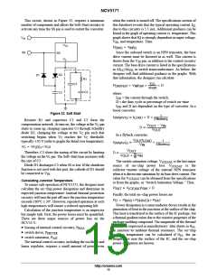
One simple method to ensure adequate phase margin is to
assuming 100% energy transfer efficiency. In continuous
conduction mode, inductor ripple current is
design the frequency response with a −20 dB per decade
slope, until unity−gain crossover. The crossover frequency
should be selected at the midpoint between f and f where
the phase margin is maximized.
V
(V
* V
)
Z1
P2
CC OUT
CC
I
+
RIPPLE
(f)(L)(V
OUT)
where:
f = 280 kHz.
f
P1
The peak inductor current is equal to average current plus
half of the ripple current, which should not cause inductor
saturation. The above equation can also be referenced when
selecting the value of the inductor based on the tolerance of
the ripple current in the circuits. Small ripple current
provides the benefits of small input capacitors and greater
output current capability. A core geometry like a rod or
barrel is prone to generating high magnetic field radiation,
but is relatively cheap and small. Other core geometries,
such as toroids, provide a closed magnetic loop to prevent
EMI.
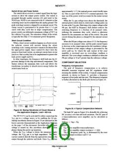
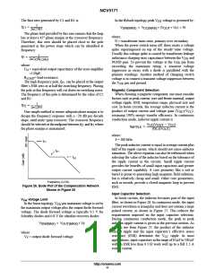
f
Z1
f
P2
Frequency (LOG)
Figure 26. Bode Plot of the Compensation Network
Shown in Figure 25
Input Capacitor Selection
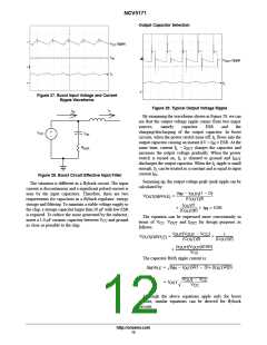
In boost circuits, the inductor becomes part of the input
filter, as shown in Figure 28. In continuous mode, the input
current waveform is triangular and does not contain a large
pulsed current, as shown in Figure 27. This reduces the
requirements imposed on the input capacitor selection.
During continuous conduction mode, the peak to peak
inductor ripple current is given in the previous section. As
we can see from Figure 27, the product of the inductor
current ripple and the input capacitor’s effective series
VSW Voltage Limit
In the boost topology, V pin maximum voltage is set by
the maximum output voltage plus the output diode forward
voltage. The diode forward voltage is typically 0.5 V for
Schottky diodes and 0.8 V for ultrafast recovery diodes
SW
V
+ V )V
OUT(MAX) F
SW(MAX)
where:
V = output diode forward voltage.
resistance (ESR) determine the V
ripple. In most
CC
F
applications, input capacitors in the range of 10 mF to 100 mF
with an ESR less than 0.3 W work well up to a full 1.5 A
switch current.
http://onsemi.com
11

 ONSEMI [ ONSEMI ]