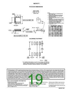
NCV5171
transitions that can cause problems. Therefore the following
guidelines should be followed in the layout.
T + T )(P q
)
J
A
D JA
where:
T = IC or FET junction temperature (°C);
A
1.
In boost circuits, high AC current circulates within the
loop composed of the diode, output capacitor, and
on−chip power transistor. The length of associated
traces and leads should be kept as short as possible. In
the flyback circuit, high AC current loops exist on both
sides of the transformer. On the primary side, the loop
consists of the input capacitor, transformer, and
on−chip power transistor, while the transformer,
rectifier diodes, and output capacitors form another
loop on the secondary side. Just as in the boost circuit,
all traces and leads containing large AC currents
should be kept short.
Separate the low current signal grounds from the
power grounds. Use single point grounding or ground
plane construction for the best results.
Locate the voltage feedback resistors as near the IC as
possible to keep the sensitive feedback wiring short.
Connect feedback resistors to the low current analog
ground.
J
T = ambient temperature (°C);
P = power dissipated by part in question (W);
D
q
= junction−to−ambient thermal resistance (°C/W).
JA
For the NCV5171, q =165°C/W.
Once the designer has calculated T , the question of
JA
J
whether the NCV5171 can be used in an application is
settled. If T exceeds 150°C, the absolute maximum
J
allowable junction temperature, the NCV5171 is not
suitable for that application.
If T approaches 150°C, the designer should consider
J
possible means of reducing the junction temperature.
Perhaps another converter topology could be selected to
reduce the switch current. Increasing the airflow across the
2.
3.
surface of the chip might be considered to reduce T .
A
Circuit Layout Guidelines
In any switching power supply, circuit layout is very
important for proper operation. Rapidly switching currents
combined with trace inductance generates voltage
http://onsemi.com
16

 ONSEMI [ ONSEMI ]